Illumination system for microlithography
- Summary
- Abstract
- Description
- Claims
- Application Information
AI Technical Summary
Benefits of technology
Problems solved by technology
Method used
Image
Examples
Embodiment Construction
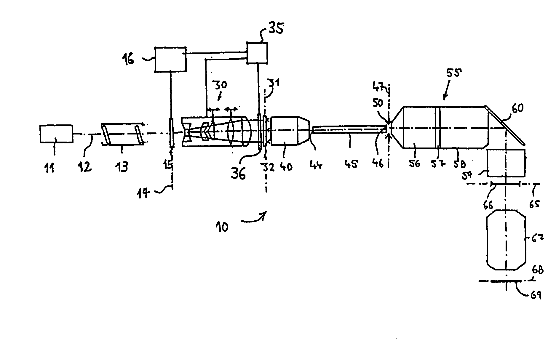
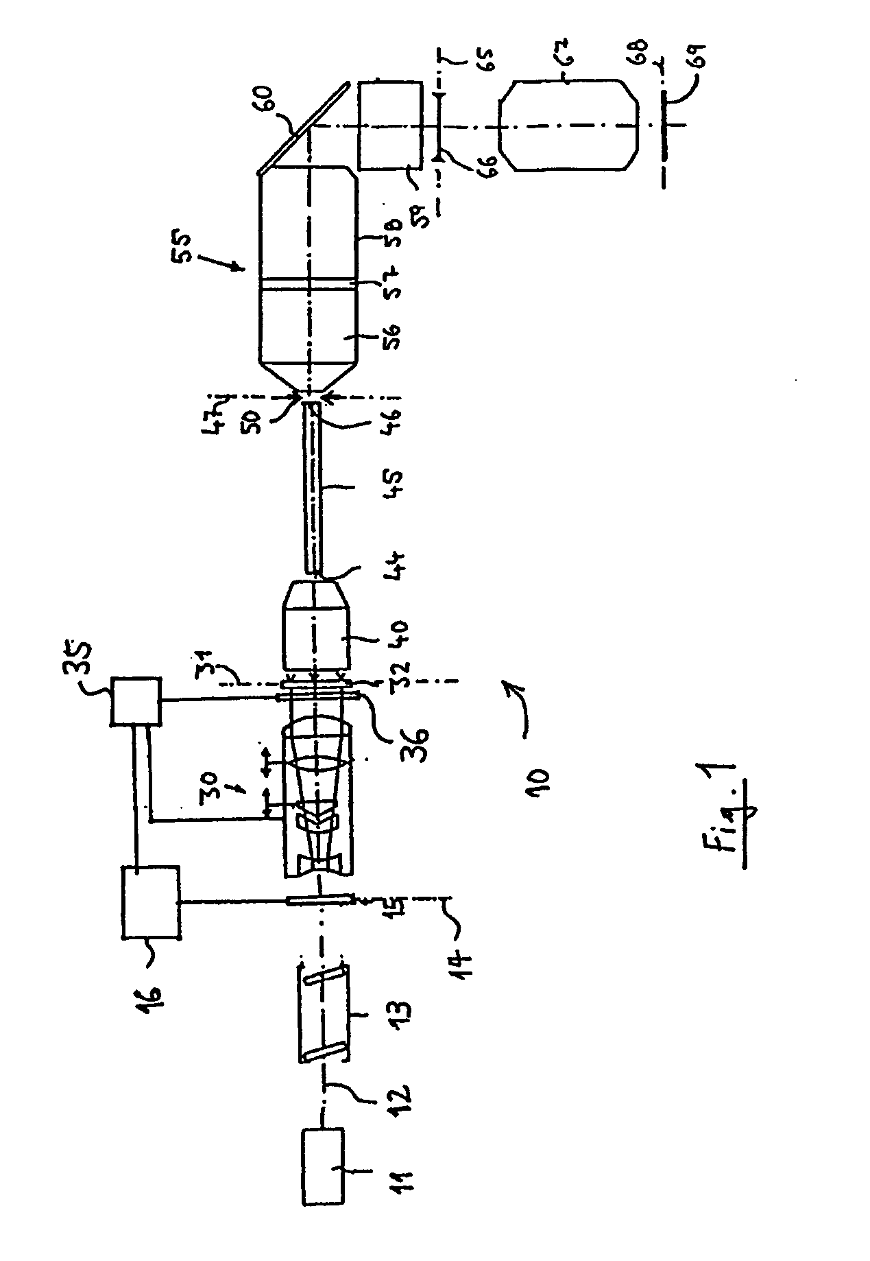
[0049]FIG. 1 shows an example of an illumination system 10 of a projection exposure apparatus for microlithography which can be used in the fabrication of semiconductor components and other finely patterned devices and operates with light from the deep ultraviolet range in order to obtain resolutions down to fractions of micrometers. The light source 11 used is an F2 excimer laser having an operating wavelength of approximately 157 nm, the light beam of which is oriented coaxially with respect to the optical axis 12 of the illumination system. Other UV light sources, for example ArF excimer lasers having an operating wavelength of 193 nm, KrF excimer lasers having an operating wavelength of 248 nm or mercury vapor lamps having an operating wavelength of 365 nm or 436 nm or light sources having wavelengths of less than 157 nm are likewise possible.
[0050] The light from the light source 11 firstly enters a beam expander 13, which expands the laser beam and forms an expanded profile w...
PUM
 Abstract
Description
Claims
Application Information
 - R&D
- Intellectual Property
- Life Sciences
- Materials
- Tech Scout
- Unparalleled Data Quality
- Higher Quality Content
- 60% Fewer Hallucinations
Browse by: Latest US Patents, China's latest patents, Technical Efficacy Thesaurus, Application Domain, Technology Topic, Popular Technical Reports.
© 2025 PatSnap. All rights reserved.Legal|Privacy policy|Modern Slavery Act Transparency Statement|Sitemap|About US| Contact US: help@patsnap.com


