
Computer automated design method, program for executing an application on a computer automated design system, and semiconductor integrated circuit

Inactive Publication Date: 2006-03-02
KK TOSHIBA
View PDF21 Cites 9 Cited by
  • Summary
  • Abstract
  • Description
  • Claims
  • Application Information

AI Technical Summary

Benefits of technology

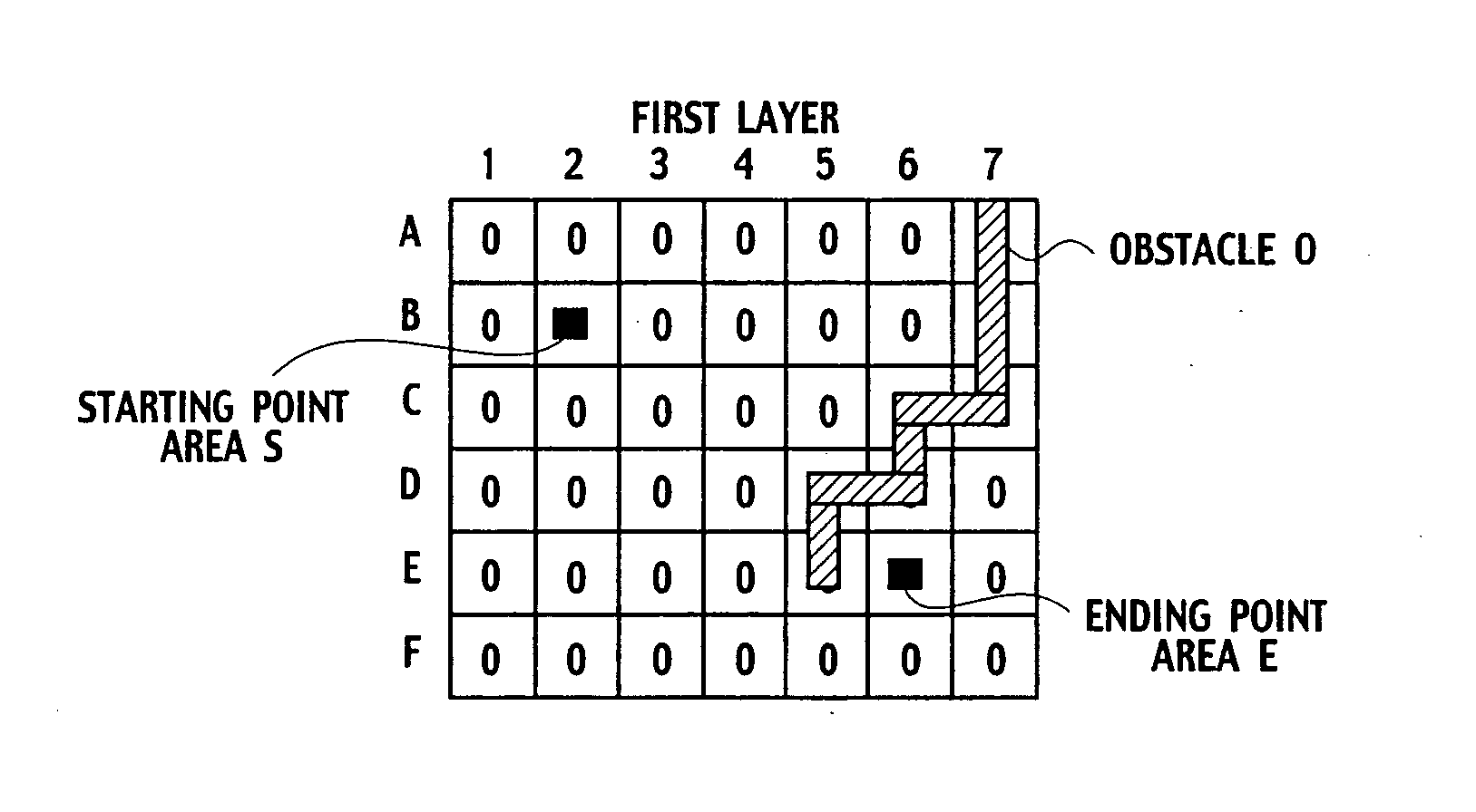
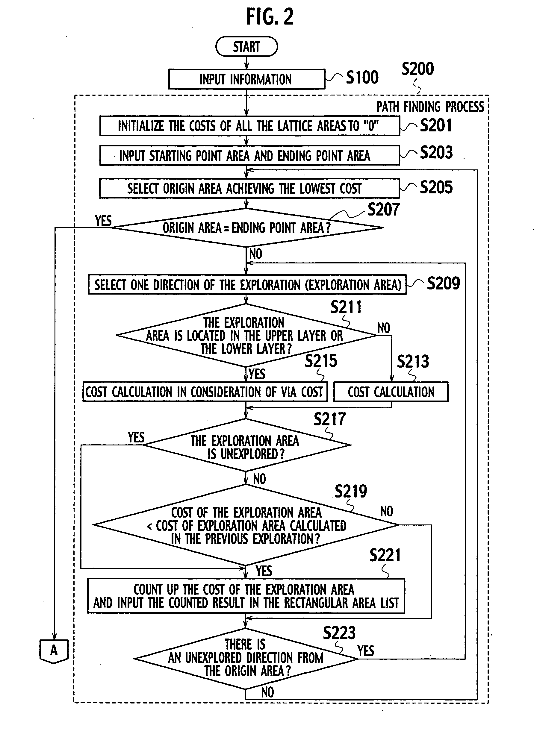
[0008] An aspect of the present invention inheres in a computer automated design method encompassing: defining rectangular areas serving as a starting point area and an ending point area of a wiring, the rectangular areas being selected from wiring areas assigned in a plurality of layers, each of layers being divided into a plurality of areas by a lattice; accumulating wiring costs by adding respective wiring cost whenever an exploration of a wiring path from the starting point area to the ending point area advances one rectangular area, multiplying the wiring cost by a via cost, when a multiple cut via is provided between the wiring areas assigned in two of the layers in the plurality of layers, and adding an obstacle cost based on obstacle information to a result of multiplication of the via cost; finding a final wiring path routing through a plurality of wiring areas in the two of layers based on a value obtained by accumulating the wiring costs to connect the starting point area and the ending point area; and arranging corresponding multiple cut via in the final wiring path connecting areas in the two of layers.
[0009] Another aspect of the present invention inheres in a program configured to be executed by a computer for executing an application on a computer automated design system, comprising: defining rectangular areas serving as a starting point area and an ending point area of a wiring, the rectangular areas being selected from wiring areas assigned in a plurality of layers, each of layers being divided into a plurality of areas by a lattice; accumulating wiring costs by adding respective wiring cost whenever an exploration of a wiring path from the starting point area to the ending point area advances one rectangular area, multiplying the wiring

Problems solved by technology

In the field of manufacturing semiconductor integrated circuits, along with increasing demands for downsizing and higher integration, it has become more difficult to form wiring shapes for connecting between elements in accordance with the original design.
Therefore, there are numerous areas in which the single cut vias cannot be replaced with the multiple cut vias due to the design, and it is not possible to improve the rate of replacement with the multiple cut vias.

Method used


Image

  • Computer automated design method, program for executing an application on a computer automated design system, and semiconductor integrated circuit
  • Computer automated design method, program for executing an application on a computer automated design system, and semiconductor integrated circuit
  • Computer automated design method, program for executing an application on a computer automated design system, and semiconductor integrated circuit

Examples


first embodiment

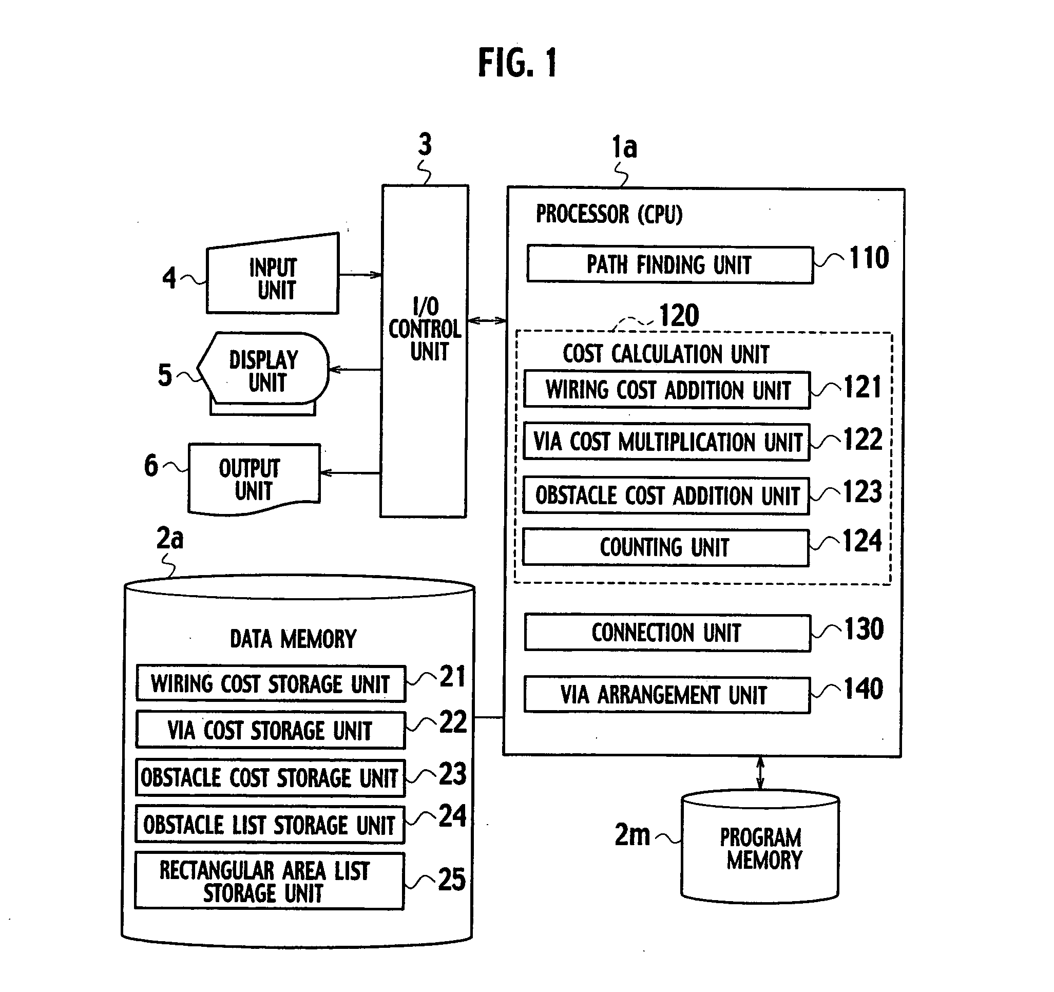
[0026] As shown in FIG. 1, a computer automated design system according to a first embodiment of the present invention includes an input unit 4 which inputs information such as data or instructions from an operator, a central processing unit (CPU) 1a which executes various calculations such as layout design, a display unit 5 and an output unit 6 which output a layout result and the like, a data memory 2a which stores given data and the like necessary for layout design of a semiconductor integrated circuit, and a program memory 2m which stores a layout program and the like for the semiconductor integrated circuit. The input unit 4, the display unit 5, and the output unit 6 are connected to the CPU 1a through an input and output control unit 3.

[0027] The CPU 1a automatically provides lines in a plurality of layers and vias for connecting between the lines onto a chip area of a semiconductor integrated circuit which is located virtually inside a memory space of the computer automated ...

second embodiment

[0078] As shown in FIG. 14, a computer automated design system according to a second embodiment of the present invention includes an input unit 4 which inputs information such as data or instructions from an operator, a central processing unit (CPU) 1b which executes various calculations such as layout design, a display unit 5 and an output unit 6 which outputs a layout result and the like, a data memory 2b which stores given data and the like necessary for layout design of a semiconductor integrated circuit, and a program memory 2n which stores a layout program and the like for the semiconductor integrated circuit. The input unit 4, the display unit 5, and the output unit 6 are connected to the CPU 1b through an input and output control unit 3.

[0079] A CPU 1b includes a path finding unit 110, a cost calculation unit 120, a connection unit 130, a via arrangement unit 140, a chip area division unit 151, a congestion degree calculation unit 152, and a congestion degree judgment unit ...

third embodiment

[0112] As shown in FIG. 21, a computer automated design system according to a third embodiment of the present invention includes an input unit 4 which accepts inputs such as data or instructions from an operator, a CPU 1c which executes various calculations such as layout design, a display unit 5 and an output unit 6 which output a layout result and the like, a data memory 2c which stores given data and the like necessary for the layout design of a semiconductor integrated circuit, and a program memory 2o which stores a layout program and the like for the semiconductor integrated circuit. The input unit 4, the display unit 5, and the output unit 6 are connected to the CPU 1c through an input and output control unit 3. The CPU 1c includes a path finding unit 110, a cost calculation unit 120, a connection unit 130, a via arrangement unit 140, a small area division unit 160, a replacement rate calculation unit 161, and a rewiring unit 162.

[0113] As shown in FIG. 23, the small area div...


PUM


Abstract

A computer automated design method includes defining rectangular areas serving as a starting point area and an ending point area of a wiring; accumulating wiring costs whenever an exploration of a wiring path from the starting point area to the ending point area advances one rectangular area, multiplying the wiring cost by a via cost and adding an obstacle cost; finding a final wiring path routing through a plurality of wiring areas to connect the starting point area and the ending point area; and arranging the corresponding multiple cut via.

Description

CROSS REFERENCE TO RELATED APPLICATIONS AND INCORPORATION BY REFERENCE [0001] This application is based upon and claims the benefit of priority from the prior Japanese Patent Applications No. P2004-244069, filed on Aug. 24, 2004; the entire contents of which are incorporated herein by reference. BACKGROUND OF THE INVENTION [0002] 1. Field of the Invention [0003] The present invention relates to a layout design methodology for a semiconductor integrated circuit, more specifically to a layout design methodology for wiring processes. [0004] 2. Description of the Related Art [0005] In the field of layout design of semiconductor integrated circuits, a maze routing is known as a method of obtaining a wiring path between two points. The maze routing is a wiring path finding method configured to set a grid (lattice) on a plane subject to wiring, and to find a path for connecting between two rectangular areas which are divided by the grid. Even when there is an obstacle such as an existing l...

Claims


Application Information

Patent Timeline
IPC IPC(8): G06F17/50
CPCG06F17/5077G06F30/394
Inventor NAKANO, MIKIO
Owner KK TOSHIBA
Learn More