
Delay line off-state control with power reduction

a delay line and power reduction technology, applied in the field of semiconductor memory devices, can solve the problems of device degradation, duty cycle errors, and device density, and achieve the effect of power reduction and power reduction

Active Publication Date: 2006-03-02
MICRON TECH INC
View PDF11 Cites 33 Cited by
  • Summary
  • Abstract
  • Description
  • Claims
  • Application Information

AI Technical Summary

Benefits of technology

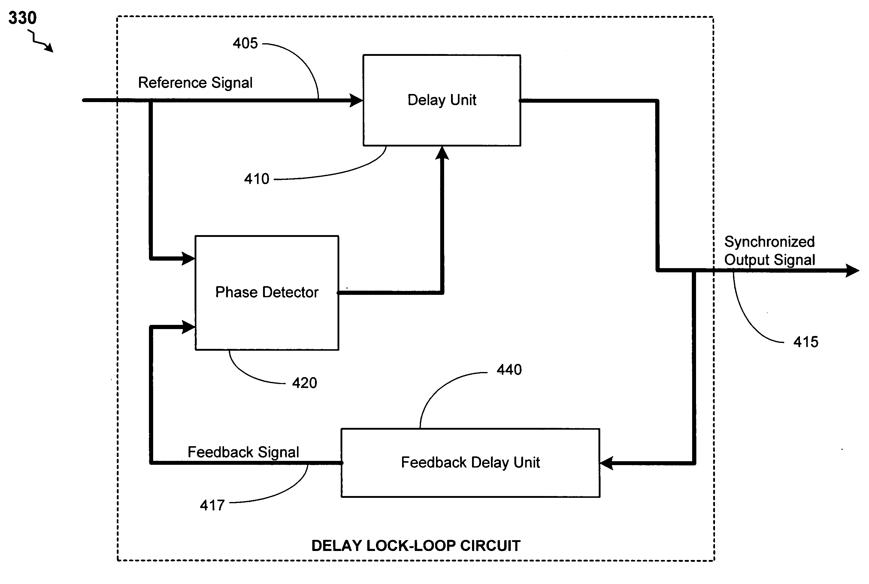
[0016] In one aspect of the instant invention, a device is provided for controlling a delay line for achieving power reduction. The device comprises a delay lock loop to provide an output signal based upon a phase difference between a reference signal and a feedback signal, said delay lock loop comprising at least one delay circuit comprising a plurality of logic gates configured to provide for substantially uniform degradation of a plurality of NAND gates in a static state.
[0017] In another aspect of the instant invention, a delay lock loop is provided for controlling a delay line for achieving power reduction. The delay lock loop provides an output signal, a feedback delay unit and a phase detector. The output signal is based upon a phase difference between a reference signal and a feedback signal. The delay lock loop comprises a delay unit. The delay unit comprises at least one delay element that is adapted to provide a delay upon at least one of a reference signal and the output signal. The delay unit comprises a plurality of logic gates configured to provide for substantially uniform degradation of a plurality of NAND gates in a static state. The feedback delay unit provides a delay upon the output signal to generate the feedback signal. The phase detector recognizes a phase difference between the reference signal and the feedback signal.
[0018] In another aspect of the instant invention, a memory device is provided which controls a delay line for achieving power reduction. The memory device comprises a delay lock loop to provide an output signal based upon a phase difference between a reference signal and a feedback signal. The delay lock loop comprises at least one delay circuit comprising a plurality of logic gates configured to provide for substantially uniform degradation of a plurality of NAND gates in a static state.
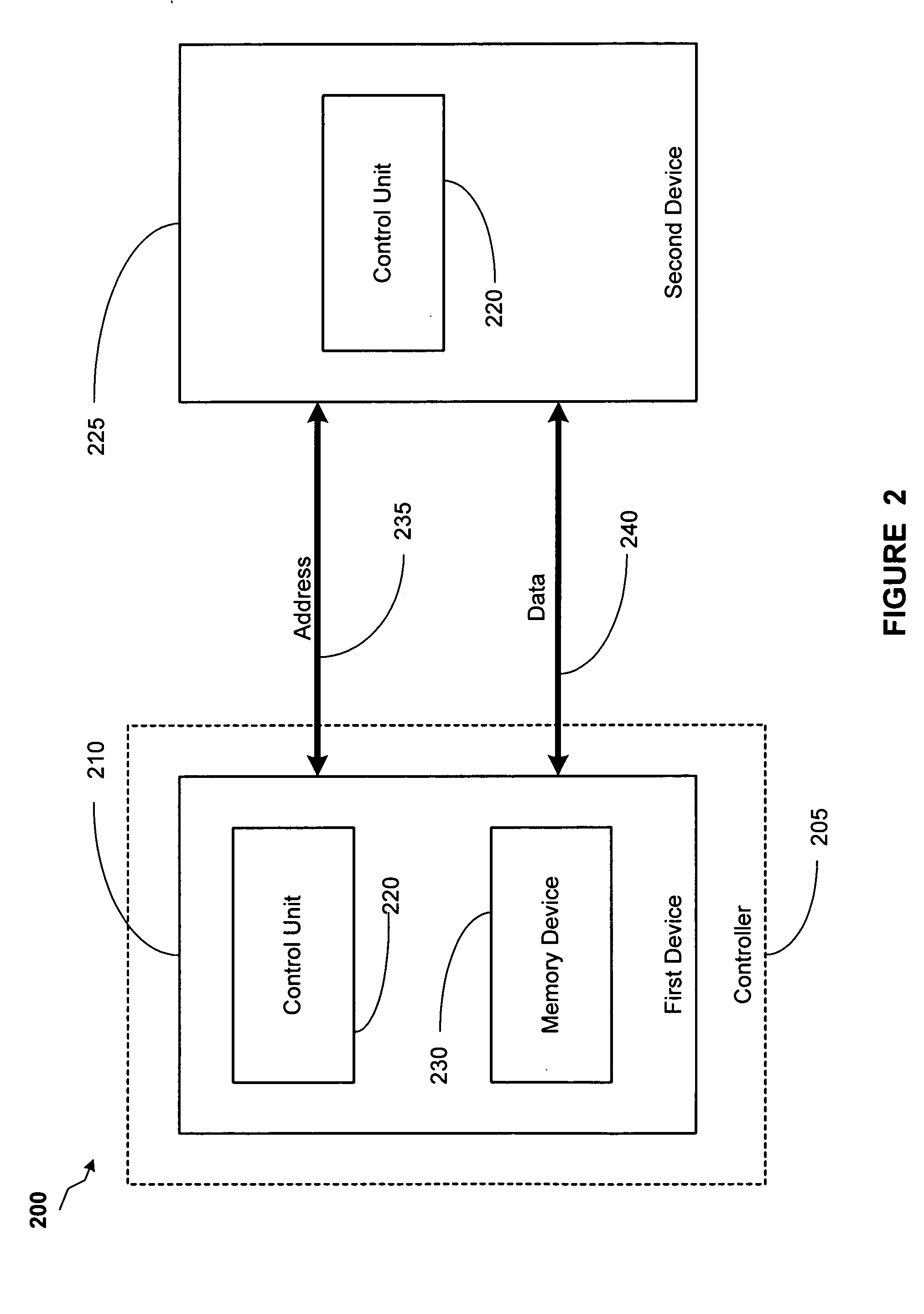
[0019] In yet another aspect of the instant invention, a system board is provided which controls a delay line for achieving power reduction. The system board comprises a first device operatively coupled to a second device. The first device comprises a memory location for storing data and a delay lock loop to provide an output signal based upon a phase difference between a reference signal and a feedback signal. The delay lock loop comprises at least one delay circuit comprising a plurality of logic gates configured to provide for substantially uniform degradation each NAND in a NAND-NAND pair. The second device is operatively coupled to the first device. The second device accesses data from the first device based upon an operation performed by the delay lock loop.

Problems solved by technology

These devices are very densely packed, i.e., there is little space between them.
However, when applying these types of delay elements, device degradation may occur.
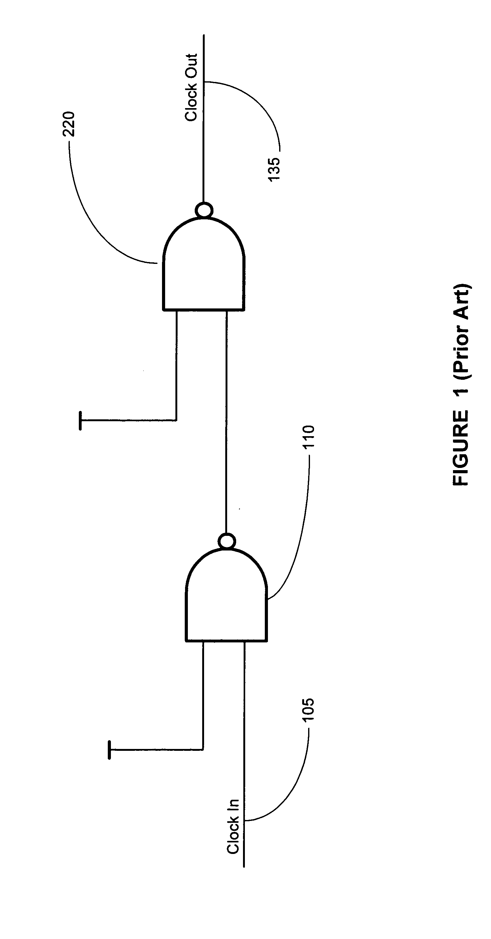
However, due to the variations in degradation, one NAND gate may degrade differently from another NAND gate, and therefore, duty cycle errors may occur.
If there were a slight duty cycle problem, for example, a pair of NAND gate fundamentally propagating the rising edges faster than the low-going edges, a cumulative effect due to the slight duty cycle error may occur.
If this duty cycle problem were to occur in multiple NAND gates, a large duty cycle error may occur.
Therefore, one problem associated with using the NAND-to-NAND topology may be that different propagation delays resulting from a signal transition from high to low time in the NAND versus an inverter may occur.
However, due to the degradation of various NAND gates, the assumptions provided in Equations 1, 2, and 3, may not hold true.
Therefore, this phenomenon may cause a duty cycle error between the difference in the clock IN on the line 105 and the clock OUT on the line 135.
However, this creates a problem with dynamic clock applications.
If the clock frequency is changed, the additional delay error may change also, leaving the possibility of continued duty cycle errors.

Method used


Image

  • Delay line off-state control with power reduction
  • Delay line off-state control with power reduction
  • Delay line off-state control with power reduction

Examples


Embodiment Construction

[0030] Illustrative embodiments of the invention are described below. In the interest of clarity, not all features of an actual implementation are described in this specification. It will of course be appreciated that in the development of any such actual embodiment, numerous implementation-specific decisions must be made to achieve the developers' specific goals, such as compliance with system-related and business-related constraints, which will vary from one implementation to another. Moreover, it will be appreciated that such a development effort might be complex and time-consuming, but would nevertheless be a routine undertaking for those of ordinary skill in the art having the benefit of this disclosure.

[0031] Synchronization between multiple digital signals in a digital system is important for accurate exchange of digital data. Often, delay lock loops are employed to synchronize digital signals. For example, a NAND gate that has a static high state applied to one input may de...


PUM


Abstract

A method and apparatus is provided for controlling a delay line for achieving power reduction. The device comprises a delay lock loop to provide an output signal based upon a phase difference between a reference signal and a feedback signal, said delay lock loop comprising at least one delay circuit comprising a plurality of logic gates configured to provide for substantially uniform degradation of a plurality of NAND gates in a static state.

Description

BACKGROUND OF THE INVENTION [0001] 1. Field of the Invention [0002] This invention relates generally to a semiconductor memory device, and, more specifically, to controlling a delay line for achieving power reduction. [0003] 2. Description of the Related Art [0004] Modern integrated circuit devices are comprised of millions of semiconductor devices, e.g., transistors, formed above a semiconductor substrate, such as silicon. These devices are very densely packed, i.e., there is little space between them. Similarly densely packed electrically conducting lines may also be formed in the semiconductor substrate. By forming selected electrical connections between selected semiconductor devices and selected conducting lines, circuits capable of performing complex functions may be created. For example, bits of data may be stored by providing electrical current to a plurality of bit lines and an orthogonal plurality of word lines that may be electrically coupled to one or more capacitors in ...

Claims


Application Information

Patent Timeline
Patent Type & Authority Applications(United States)
IPC IPC(8): H03L7/00
CPCG11C7/22H03L7/0814H03L7/0802G11C7/222H03L7/0816H03L7/0818
Inventor GOMM, TYLER J.BELL, DEBRA
Owner MICRON TECH INC
Learn More