
Generation and measurement of timing delays by digital phase error compensation

a phase error compensation and timing delay technology, applied in time-delay networks, multi-port active networks, instruments, etc., can solve the problems of timing uncertainty relating to temporal difference, timing uncertainty, inherent timing uncertainty, etc., and achieve the effect of improving the synchronization of outputs

Inactive Publication Date: 2006-02-23
REILLY JAMES P +1
View PDF14 Cites 20 Cited by
  • Summary
  • Abstract
  • Description
  • Claims
  • Application Information

AI Technical Summary

Benefits of technology

[0020] Further illustratively according to this aspect of the invention, the apparatus comprises a synchronization circuit coupled to the field programmable gate array for improving the synchronization of the outputs of the field programmable gate array.
[0053] Further illustratively according to this aspect of the invention, the apparatus comprises a synchronization circuit coupled to the field programmable gate array for improving the synchronization of the outputs of the field programmable gate array.

Problems solved by technology

When the trigger signal is received at a random time between the master clock pulses, there is inherent timing uncertainty.
This timing uncertainty, commonly called jitter, is caused from the triggering event not being related in phase to the master clock.
In particular, the timing uncertainty relates to the temporal difference between the trigger signal and the master clock pulse.
Therefore, the timing uncertainty relates to the period of the master clock.
However, increasing the speed of the master clock typically comes at the expense of increased circuit complexity and cost.
Additionally, there are practical limits to the speed of a master clock.
However, one terahertz clocks are not practical with currently available technology.

Method used


Image

  • Generation and measurement of timing delays by digital phase error compensation
  • Generation and measurement of timing delays by digital phase error compensation
  • Generation and measurement of timing delays by digital phase error compensation

Examples


Embodiment Construction

[0080] While the disclosure is susceptible to various modifications and alternative forms, specific embodiments thereof have been shown by way of example in the drawings and will herein be described in detail. It should be understood, however, that there is no intent to limit the disclosure to the particular forms disclosed, but on the contrary, the disclosure is to cover all modifications, equivalents, and alternatives falling within the spirit and scope of the disclosure as defined by the appended claims.

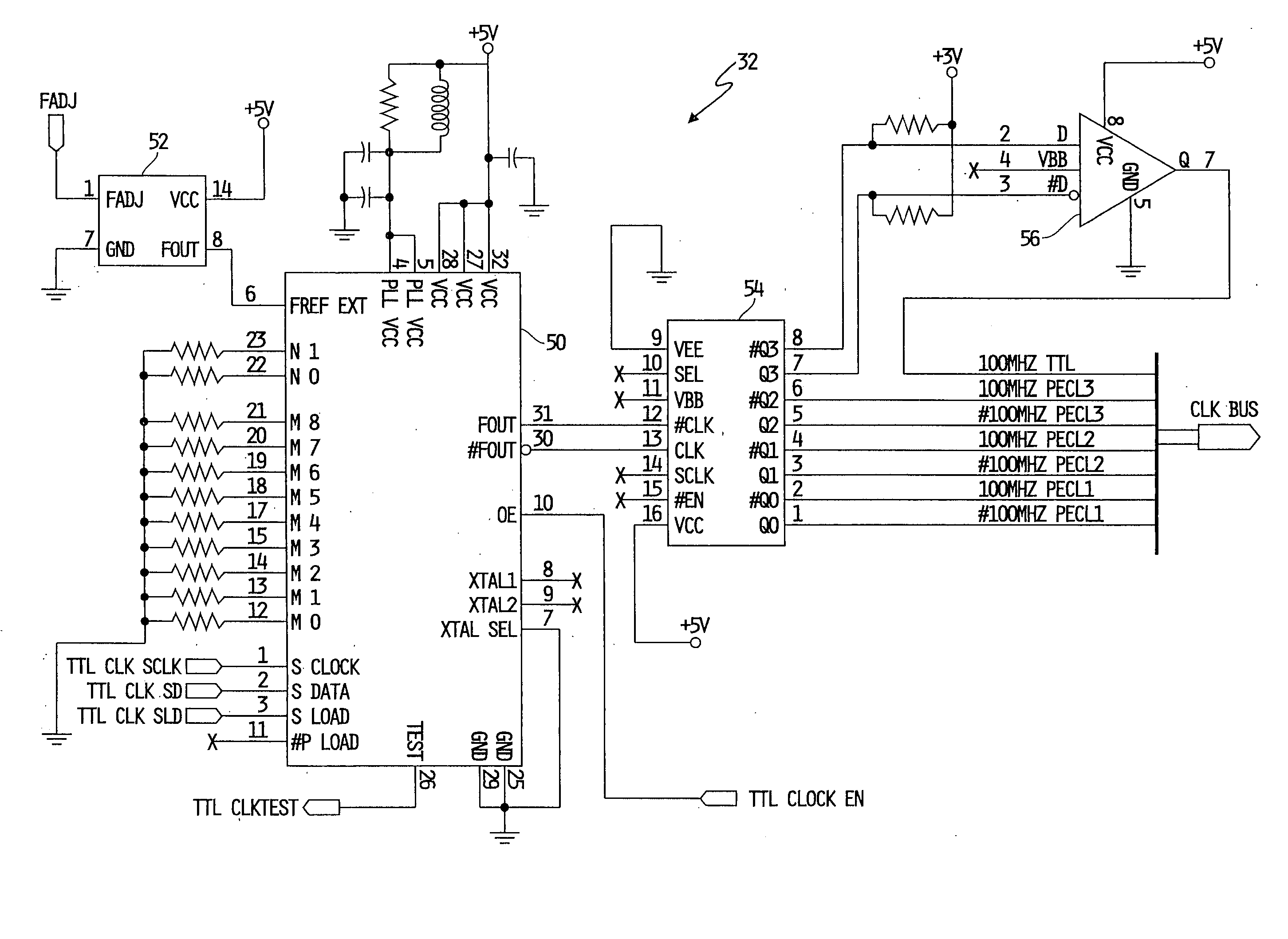
[0081] In the detailed descriptions that follow, several integrated circuits and other components are identified, with particular circuit types and sources. In many cases, terminal names and pin numbers for these specifically identified circuit types and sources are noted. This should not be interpreted to mean that the identified circuits are the only circuits available from the same, or any other, sources that will perform the described functions. Other circuits are typically a...


PUM


Abstract

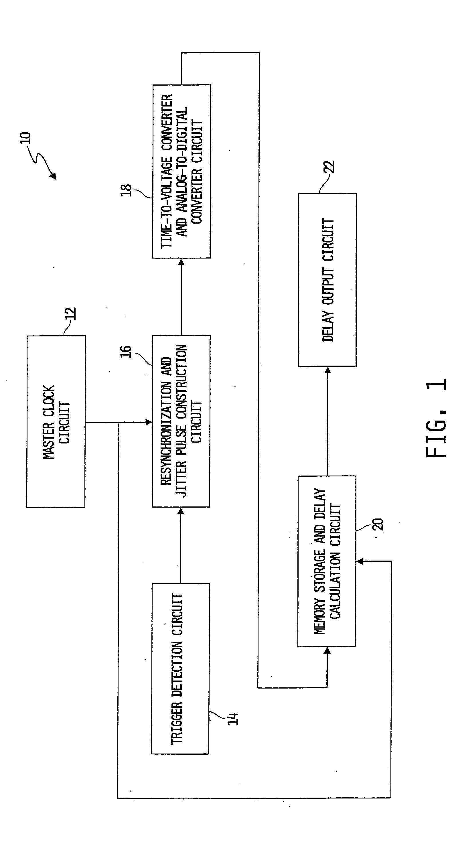
A circuit and method for generating a delayed event following a trigger pulse occurring at a random time between clock pulses is disclosed. The circuit includes a clock circuit, a voltage converter, an analog-to-digital converter circuit, a memory storage circuit, and a summing circuit. The method includes representing the time between the triggering pulse and a subsequent clock pulse as a voltage, converting the voltage to a stored digital value, and defining a desired delay time by adding a first time determined by counting a predetermined number of clock cycles to a second time determined by converting the stored digital value first to an analog value and then to a time value.

Description

[0001] This application is a divisional of U.S. patent application Ser. No. 10 / 744,834 filed Dec. 23, 2003, which claims priority under 35 U.S.C. § 119(e) to U.S. Provisional Application Ser. No. 60 / 455572, filed on Mar. 17, 2003, the disclosure of both which are hereby incorporated by reference herein.FIELD OF THE INVENTION [0002] This invention relates generally to apparatus and methods for the generation of events following a trigger pulse. It is disclosed in the context of an electronic circuit and method for the generation of events following a trigger pulse when the trigger pulse occurs at an indeterminate time between clock pulses. However, it is believed to be useful in other applications as well. BACKGROUND OF THE INVENTION [0003] The generation of events following an input trigger pulse is a common requirement in electrical applications. Generally, a timing delay generator receives a trigger signal and counts pulses of an internally generated master clock to generate a kno...

Claims


Application Information

Patent Timeline
Patent Type & Authority Applications(United States)
IPC IPC(8): H03H11/26G01R31/30G01R31/317G01R31/3193
CPCG01R31/3016G01R31/31937G01R31/31725
Inventor REILLY, JAMES P.CHRISTIAN, NOAH P.
Owner REILLY JAMES P
Learn More