
System of detection and repair and method thereof

a technology system, applied in the direction of electric discharge tube/lamp manufacture, semiconductor/solid-state device testing/measurement, multi-layer pixel stacking abnormally, etc., can solve the problems of short circuit, electrodes of organic electroluminescent apparatus may contact each other, defects may be undetected, etc., to achieve the effect of reducing waste of manpower sources, detecting quickly and correctly, and efficiently repairing defects

Inactive Publication Date: 2006-02-09
RITDISPLAY
View PDF5 Cites 16 Cited by
  • Summary
  • Abstract
  • Description
  • Claims
  • Application Information

AI Technical Summary

Benefits of technology

[0013] In view of the foregoing, the invention is to provide a system and a method of detection and repair, which can efficiently detect and repair the defect(s) of an organic electroluminescent apparatus.
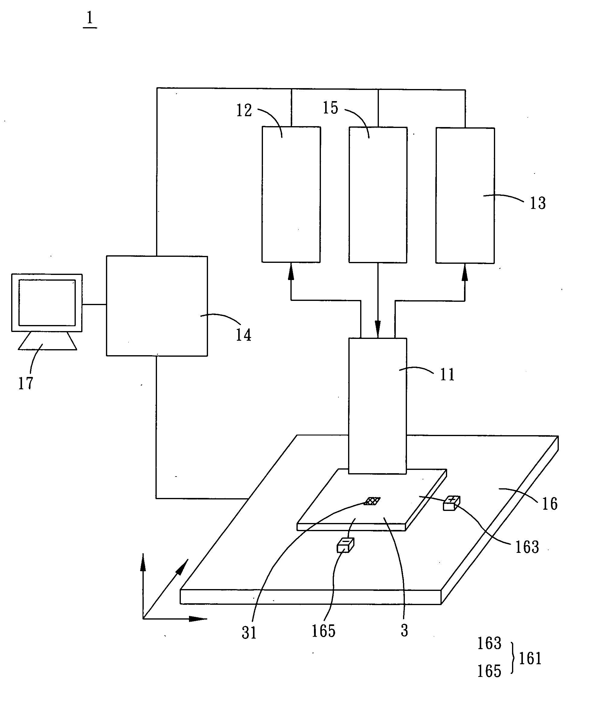
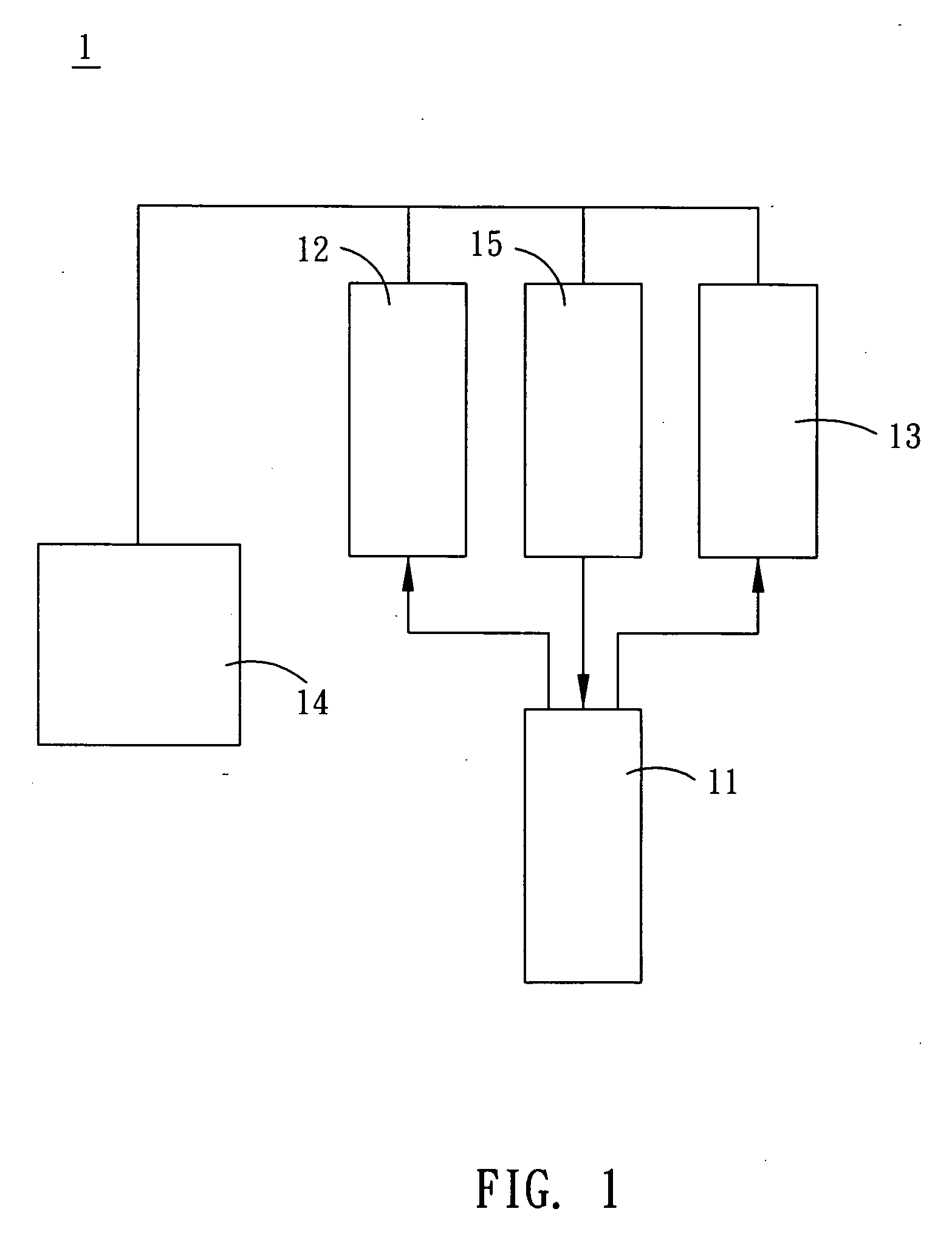
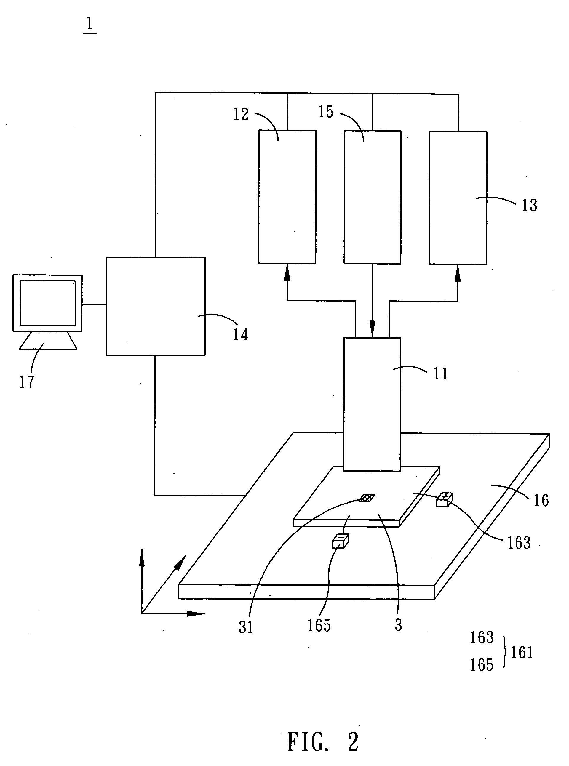
[0018] As mentioned above, the system and method of detection and repair of the invention, in advance, uses the microscope and image-retrieving device to enlarge and retrieve the image of the detected region on the organic electroluminescent apparatus, or uses the precise distance measurement device and controller to automatically adjust the relative positions of the organic electroluminescent apparatus and the current detector or the distance therebetween. Then, the detected region of the organic electroluminescent apparatus is charged with a bias, so that the current detector can detect the location of the defect having abnormal current distribution. Finally, the beam is generated to isolate the defect. Therefore, it is unnecessary to apply a conventional detection machine and a conventional repairing machine to perform the detecting and repairing processes. Besides, the organic electroluminescent apparatus to be detected and repaired can be automatically aligned. Thus, the possible errors caused by artificial operations and the waste of manpower sources can be efficiently reduced. Moreover, the invention is to detect the abnormal current distribution for detecting the location of the defect, so that the location of the defect can be found out quickly and correctly. As a result, the defects of the organic electroluminescent apparatus can be detected and repaired efficiently.

Problems solved by technology

If particles exist on a pixel of the organic electroluminescent apparatus during manufacture thereof, the multiple layers of the pixel may be stacked abnormally.
Additionally, the electrodes of the organic electroluminescent apparatus may contact each other and short-circuit.
However, this check method is by manpower and is time consumptive, and some defects may be undetected due to artificial carelessness.
In practice, the detected defect(s) of the organic electroluminescent apparatus cannot be repaired directly because the organic electroluminescent apparatus is transported from the detection machine to the repairing machine.
As mentioned above, a foreign particle exists on the pixel may induce the stacking problem, and further induce a short circuit.
However, the defect caused by this particle can be ignored and is unnecessary to be repaired if the particle is smaller than a certain size and the short-circuited issue does not occur.
This method, however, cannot determine whether the defect will cause the short-circuited issue or not, and as a result, all detected defects will be repaired during the repairing process.
In other words, the conventional technology will scan an organic electroluminescent apparatus, locate defects, scan the device again, locate the defects again, and then repair all the detected defects, resulting in wasting time and resources in the manufacturing processes.

Method used


Image

  • System of detection and repair and method thereof
  • System of detection and repair and method thereof
  • System of detection and repair and method thereof

Examples


Embodiment Construction

[0026] The present invention will be apparent from the following detailed description, which proceeds with reference to the accompanying drawings, wherein the same references relate to the same elements.

[0027] The system and method of detection and repair according to the preferred embodiments of the invention will be described herein below with reference to the accompanying drawings, wherein the same reference numbers refer to the same elements. To be noted, the organic electroluminescent apparatuses described in the following comprise organic electroluminescent panels and organic electroluminescent devices.

[0028] With reference to FIG. 1 and FIG. 2, a system of detection and repair 1 according to a preferred embodiment of the invention comprises a microscope 11, an image-retrieving device 12, a current detector 13, a controller 14, and a beam generator 15.

[0029] The microscope 11 is used to enlarge an image of a detected region in an organic electroluminescent apparatus 3. The ...


PUM


Abstract

A system of detection and repair is to detect and repair an organic electroluminescent apparatus. When detecting locations of defects, the system charges a bias to the detected locations of the organic electroluminescent apparatus. A detector, such as an infrared (IR) detector, of the system detects the locations of defects having abnormal current distribution. A beam generator of the system is then used to generate a beam for isolating the defects. A method of detection and repair is further provided.

Description

BACKGROUND OF THE INVENTION [0001] 1. Field of Invention [0002] The invention relates to a system and a method of detection and repair and, in particular, to a system and method for detecting and repairing defects of an organic electroluminescent apparatus. [0003] 2. Related Art [0004] Information communication technology has become a major focus of the industry, especially the portable communication display products which are the point of development. Flat panel displays provide an interface between humans and information, thus they have become an important development direction of manufacturers. Present choices of flat panel displays include the plasma display panel (PDP), liquid crystal display (LCD), inorganic electroluminescence display (ELD), light-emitting diode (LED) display, vacuum fluorescence displays (VFD), field emission displays (FED), electro-chromic display, and the likes. [0005] Compared to other flat panel displays, organic electroluminescent apparatuses, such as o...

Claims


Application Information

Patent Timeline
Patent Type & Authority Applications(United States)
IPC IPC(8): G01R31/305H01J9/50G09G3/00G09G3/32H01L21/66H05B33/10
CPCG09G3/006H01L2251/568G09G3/3208H10K71/861
Inventor LIAO, MENG-CHIEHCHEN, CHI-CHUNG
Owner RITDISPLAY
Learn More