Microwave phase shifter and power amplifier
a phase shifter and power amplifier technology, applied in the direction of delay lines, waveguides, electrical apparatus, etc., can solve the problems of increasing the number of manufacturing steps, increasing the cost and complicated circuit configuration of microwave phase shifters formed on the substrate, etc., to achieve easy and precise phase shift adjustment, simple circuit configuration, and easy manufacturing cost reduction
- Summary
- Abstract
- Description
- Claims
- Application Information
AI Technical Summary
Benefits of technology
Problems solved by technology
Method used
Image
Examples
first embodiment
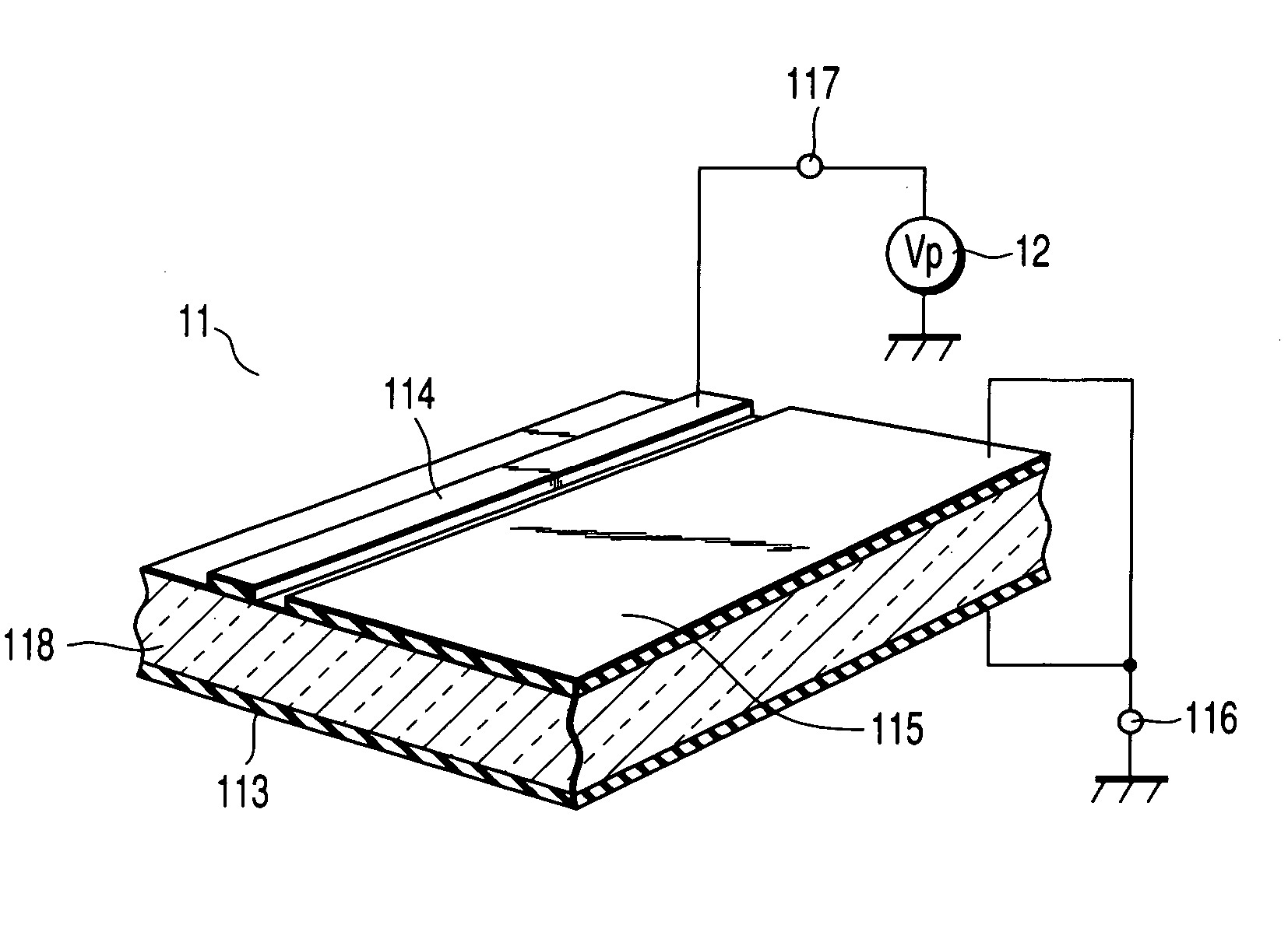
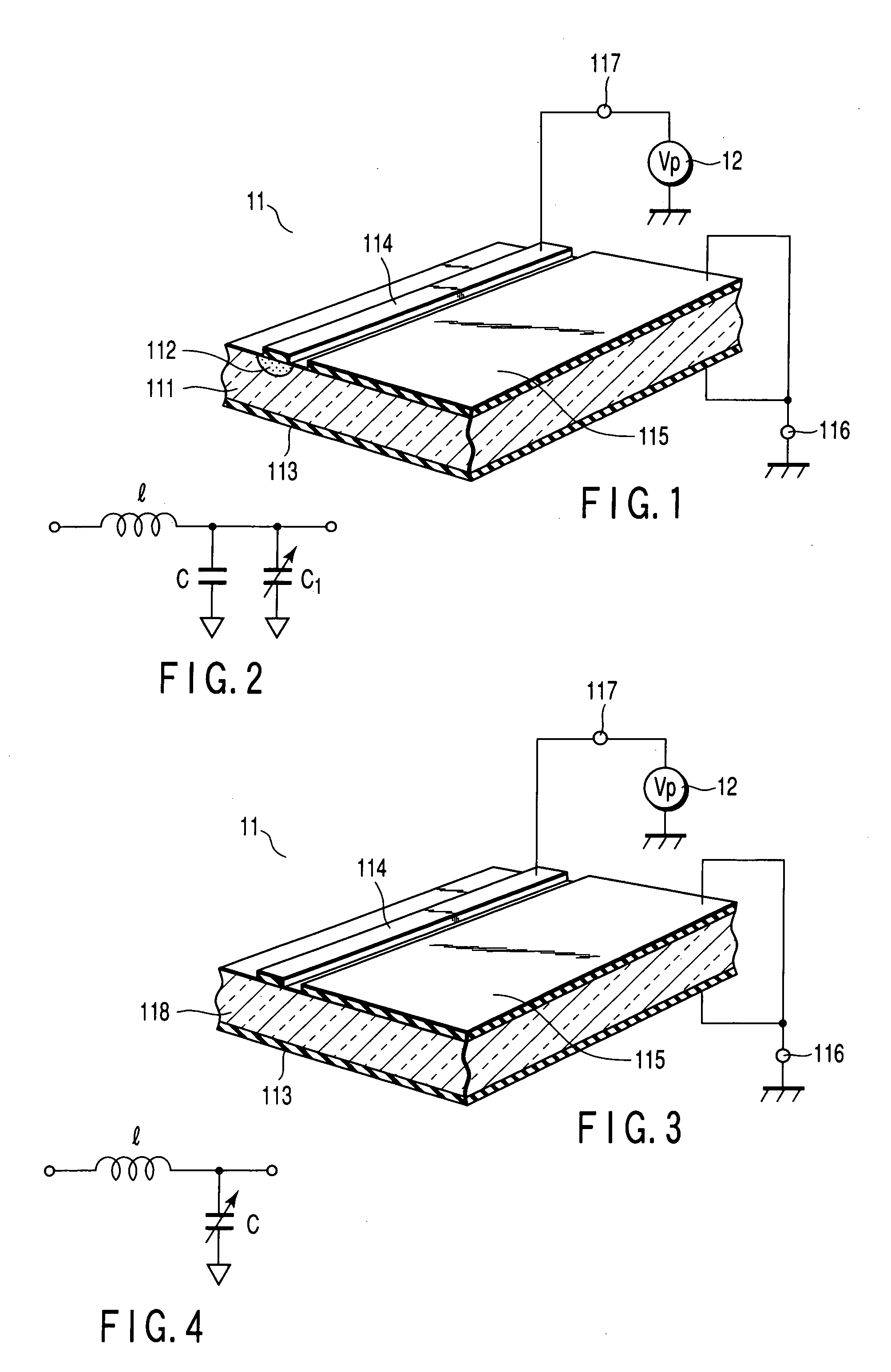
[0021]FIG. 1 is a configuration view showing the configuration of a microwave phase shifter according to a first embodiment of this invention. In FIG. 1, reference label 11 denotes a circuit board of the microwave phase shifter. The circuit board 11 is a semi-insulating substrate having a semi-insulating layer 111 formed of a semi-insulating material such as GaAs. On one surface side (front surface side of the substrate) of the semi-insulating layer 111, an active layer 112 is formed in at least a transmission line forming portion, and on the other surface side (rear surface side of the substrate), a first conductive layer 113 of a metal material is formed. The active layer 112 is formed by ion-implanting an impurity into the semi-insulating layer 111, for example.
[0022] On the upper side of the active layer 112, a transmission line 114 of a metal material is formed. Further, on the surface of the semi-insulating layer 111 on which the transmission line 114 is formed, a second cond...
second embodiment
[0031]FIG. 3 is a configuration view showing the configuration of a microwave phase shifter according to a second embodiment of this invention. In FIG. 3, the same portions as those of FIG. 1 are denoted by the same reference symbols and different portions are taken up and explained here.
[0032] A circuit board 11 shown in FIG. 3 includes a liquid crystal dielectric layer 118 instead of the semi-insulating layer of FIG. 1. Like the first embodiment, a transmission line 114 and first and second grounding conductive layers 113, 115 formed on the front surface and rear surface of the liquid crystal dielectric layer 118 configure a micro-coplanar strip line utilizing the proximity effect.
[0033] However, in the present embodiment, no active layer is formed.
[0034] With the above configuration, if bias voltage Vp is applied to the transmission line 114, voltages are applied to the liquid crystal dielectric layer 118 between the transmission line 114 and the first grounding conductive lay...
third embodiment
[0042]FIG. 5 is a block circuit diagram showing the configuration of a power amplifier according to a third embodiment of this invention. In FIG. 5, a microwave transmission signal is supplied to an input terminal 21. The signal is distributed into two paths. One of the paths is used as a reference path and the distributed signal thereof is supplied to an amplifier 23 and power-amplified. The distributed signal of the other path is phase-adjusted by a phase shifter 24 so that the phase thereof will correspond to the signal of the reference path and is then supplied to an amplifier 25 and power-amplified. The distributed signals power-amplified by the respective amplifiers 23, 25 are synthesized in a synthesizer 26 and output from an output terminal 27.
[0043] The power amplifier of the above configuration is a so-called power synthesizing type, and it evenly matches the phases when power-amplifying the distributed microwave signals and adds and synthesizes the power-amplified output...
PUM
 Abstract
Description
Claims
Application Information
 - R&D
- Intellectual Property
- Life Sciences
- Materials
- Tech Scout
- Unparalleled Data Quality
- Higher Quality Content
- 60% Fewer Hallucinations
Browse by: Latest US Patents, China's latest patents, Technical Efficacy Thesaurus, Application Domain, Technology Topic, Popular Technical Reports.
© 2025 PatSnap. All rights reserved.Legal|Privacy policy|Modern Slavery Act Transparency Statement|Sitemap|About US| Contact US: help@patsnap.com


