
Test structures and method for interconnect impedance property extraction

a technology of impedance property and test structure, which is applied in the direction of resistance/reactance/impedence, fault location, instruments, etc., can solve the problems of signal delay caused by the on-chip metal interconnect becoming significant, rc delay, and unsatisfactory actual metal interconnects

Active Publication Date: 2006-02-02
SIEMENS PROD LIFECYCLE MANAGEMENT SOFTWARE INC
View PDF12 Cites 29 Cited by
  • Summary
  • Abstract
  • Description
  • Claims
  • Application Information

AI Technical Summary

Benefits of technology

[0014] Other features and advantages of the disclosed methods and structures will be

Problems solved by technology

An ideal metal interconnect should play no active role in the integrated circuit other than conducting electrons, but actual metal interconnects are not ideal.
As the signal switching speeds exceed 1 GHz and chip densities exceed tens of millions of transistors, signal delay caused by the on-chip metal interconnects becomes significant.
However, although use of better materials may reduce the RC delay, it does not eliminate them.
In addition, these measures are less effective in reducing the delays dominated by inductance.
For example, high-speed VLSI exhibits subnanosecond switching and requires clock signal propagation bandwidth above 1 GHz in order to maintain rise times. Under such frequency ranges, the self inductance of a signal wire can create a signal-delay problem.
In addition to causing signal delay, inductance also contributes signal noise in an integrated circuit.
Signal noise and cross-talk largely relate to the mutual inductance among neighboring signal wires and may create signal-integrity problems.

Method used


Image

  • Test structures and method for interconnect impedance property extraction
  • Test structures and method for interconnect impedance property extraction
  • Test structures and method for interconnect impedance property extraction

Examples


Embodiment Construction

[0027] A. Terms

[0028] In the present description, the term “impedance” broadly encompasses any quantity that characterizes the input / output relationship such as the amount of reflection relative to transmission. For electric impedance, impedance encompasses resistance, capacitance, inductance and conductance. Under an AC condition, impedance can be a complex quantity. Any linear sinusoidal driven combination of capacitors, inductors, resistors has a steady state solution of the form

I=I0 cos(wt+φ),  (1)

[0029] which can be found using a complex impedance Z defined by Z≡VI,(2)

[0030] where for capacitors, Z≡VI=-iwC.(3)

[0031] For inductors, Z≡VI=iwL.(4)

[0032] For resistors, the impedance is simply equal to the resistance R,

Z=R.  (5)

[0033] The term “integrated circuit” has the ordinary meaning as understood in the art. An integrated circuit may be, but is not limited to, a microprocessor, an application-specific integrated circuit (ASIC), a programmable logic device (PLDs) such as a...


PUM


Abstract

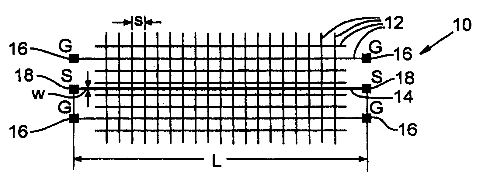
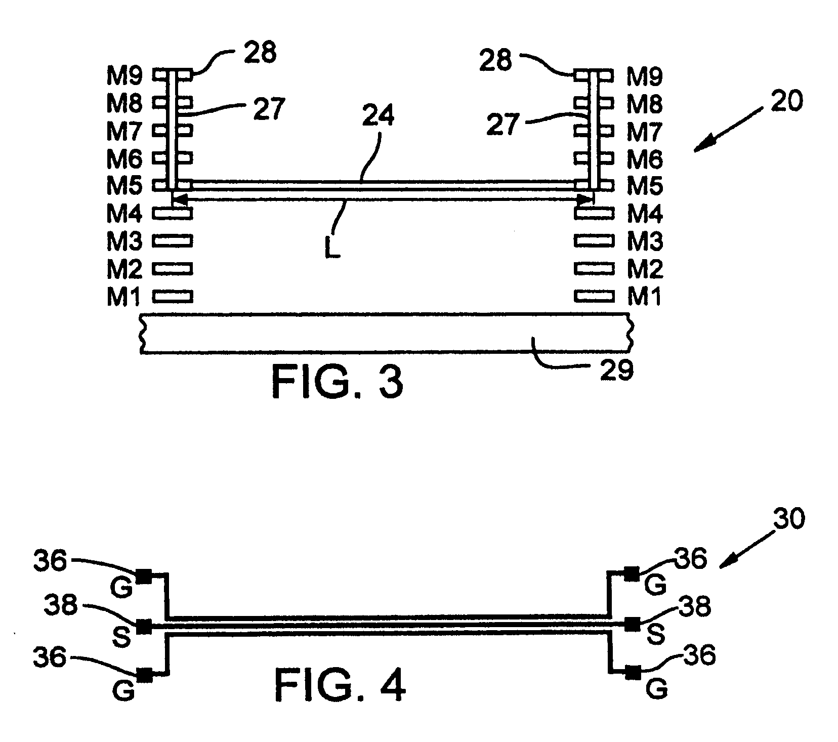
A method and test structures are disclosed for characterizing interconnects of an integrated circuit. The method provides a set of test structures and determines a unit impedance property of each test structure, desirably using S-parameter measurements. A reference impedance data set is then formulated that characterizes the impedance of an integrated circuit manufacturing technology and that can be used to characterize the impedance of interconnects of the chip made by the technology. Each test structure desirably comprises a ground grid and a signal line, and is characterized by values of a set of predetermined attributes such as layer location of the respective ground grid, grid density, layer association, width and length of the respective signal line.

Description

RELATED APPLICATION DATA [0001] This application claims the benefit of U.S. provisional patent application No. 60 / 598,703, filed Aug. 2, 2004, entitled, “Test Structures and Method for Interconnect Impedance Property Extraction”, by Hazem Hegazy, Amr M. E. Safwat, and Wael Fikry Farouk Fikry Abdalla, which is hereby incorporated by reference.BACKGROUND [0002] The present disclosure relates to techniques for extracting interconnect impedance properties, such as inductance, of an integrated circuit. [0003] Metal interconnects are an important part of integrated circuits. Partly because on-chip metal interconnects tend to be denser, faster, and more reliable than off-chip connections, there is a continuing drive toward higher levels of chip integrations. This continuing drive in turn places more and more stringent requirements on the properties of on-chip metal interconnects. [0004] Metal interconnects play several crucial roles including forming signal lines and providing networks for...

Claims


Application Information

Patent Timeline
IPC IPC(8): G01R31/08G06F17/50
CPCG01R27/28G01R31/2853H01L23/522H01L2924/0002H01L2924/00
Inventor HEGAZY, HAZEM MAHMOUDSAFWAT, AMR M.E.ABDALLA, WAEL FIKRY FAROUK FIKRY
Owner SIEMENS PROD LIFECYCLE MANAGEMENT SOFTWARE INC
Learn More