
Method for microfabricating structures using silicon-on-insulator material

a technology of silicon-on-insulator and microfabrication, which is applied in the direction of manufacturing tools, soldering devices, instruments, etc., can solve the problems of poor process control, the use of soi wafers to build mems devices is not widespread, and the method involves the use of a heavily-boron-doped etch stop

Inactive Publication Date: 2006-01-19
CHARLES STARK DRAPER LABORATORY
View PDF20 Cites 20 Cited by
  • Summary
  • Abstract
  • Description
  • Claims
  • Application Information

AI Technical Summary

Benefits of technology

[0009] The method described above is generally called Bonded and Etch Back Silicon-On-Insulator (BESOI). In the BESOI method, the structure etching is performed after the SiO2 layer is removed, so that when the handle layer is removed by wet or dry etching, the SiO2 layer is supported by the device layer, thus the SiO2 layer can function as an etch stop, and no chemicals penetrate the SiO2 layer to the device region to damage the device when the SOI wafer handle Si is removed.
[0011] The method of the invention provides (I) the ability to micromachine devices on SOI substrates without design constraints for structure spacing, etch gaps, oxide thickness or other features, and (2) a flexibility for handle wafer type and bonding process. This invention also addresses several of the previous barriers to general use of SOI material for MEMS and associated applications. First, the invention enables the use of SOI wafers to build a wide array of device types that were previously only feasible using standard boron etch stop technology. Second, the method allows for the use of RIE etch technology to produce high-quality structures on devices bonded everywhere to a silicon dioxide buried layer. Third, the invention relieves all of the design constraints previously required for SOI structures, including the spacing between structural elements, spacing between the device and the edge of the die, and special requirements for atmospheric conditions during bonding of SOI wafers to handle wafers.
[0015] In one preferred embodiment, the substrate is provided with access ports to equalize the pressure between the internal cavities and outside of the wafer sandwich. In another preferred embodiment, the process of bonding the SOI wafer and the substrate is performed at a pressure less than atmospheric pressure. Thus, some gas can be present in the cavities formed between the Si and the substrate, but the gas pressure is not great enough to cause devices to explode during a subsequent potassium hydroxide (KOH) etch to remove the handle layer. This step avoids the need for drilling holes in the substrate.

Problems solved by technology

In spite of its many advantages, however, use of SOI wafers to build MEMS devices is not widespread, largely because of difficulties in processing the material.
However, methods that involve the use of a heavily-boron-doped etch stop suffer in several respects, including poor process control, high defect densities, limitations on ultimate thickness of devices, and incompatibility with microelectronic device integration.
Insertion of a SiGe alloy layer resolves several of these limitations, but that method suffers from relatively low deposition rates and material property issues.
SOI micromachining has demonstrated that a limited number of device types may be successfully constructed, but the build quality is lacking and many design constraints exist.
The principal constraint involves the problems encountered when performing deep reactive-ion-etching (RIE) of the silicon device layer on top of the oxide interlayer; the RIE process tends to attack the underside of the silicon device layer due to charging of the dielectric layer.
However, these alternative processes encounter stringent design rules related to pressure differentials across the thin oxide interlayer.
Survival of the oxide interlayer is important for the success of alternative SOI processes, but no solution to this problem has previously been proposed.

Method used


Image

  • Method for microfabricating structures using silicon-on-insulator material
  • Method for microfabricating structures using silicon-on-insulator material
  • Method for microfabricating structures using silicon-on-insulator material

Examples


example

Fabrication Method for ALT BESOI Accelerometer

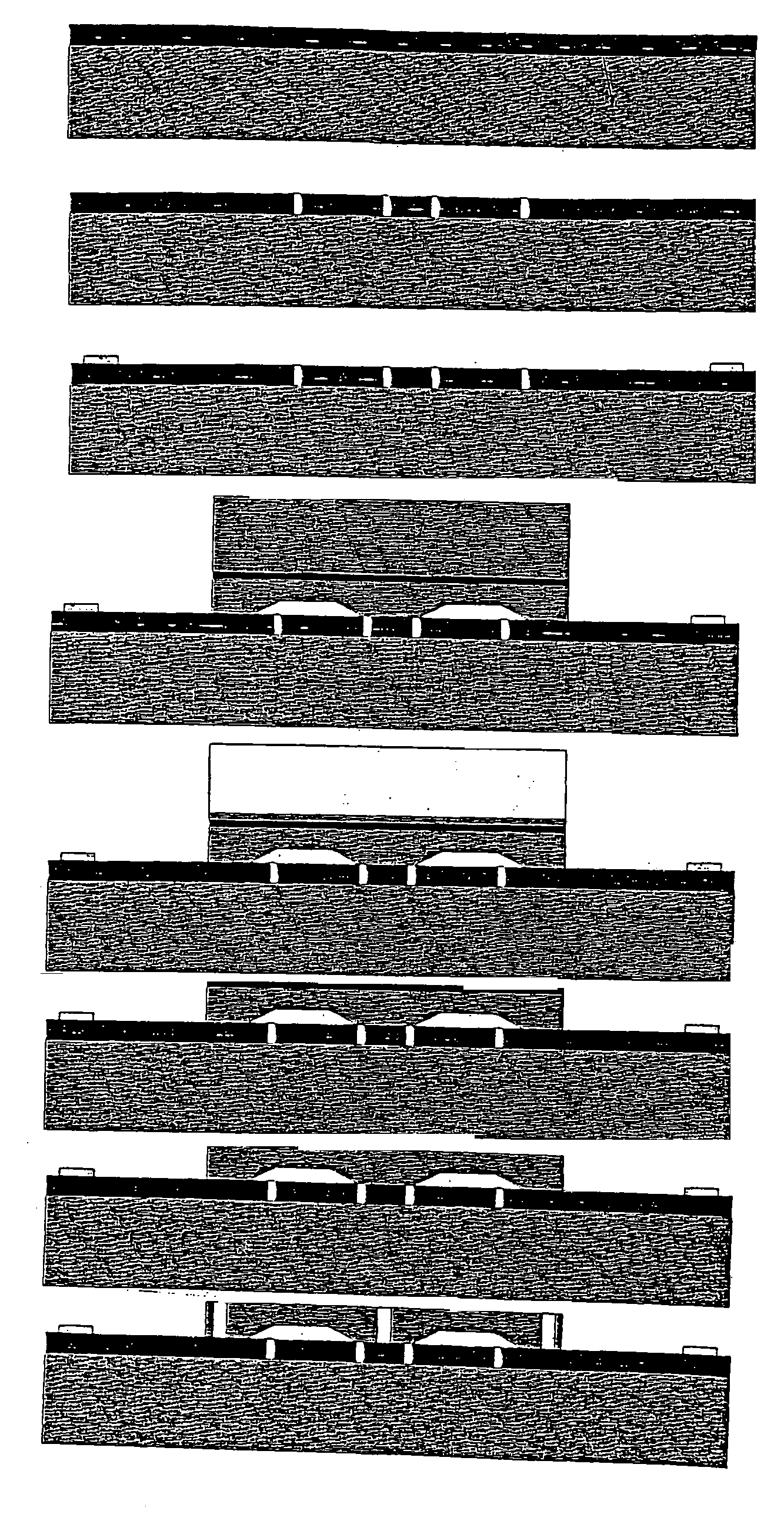
[0060] Summary. Several significant barriers to successful fabrication of the Silicon Oscillator Accelerometer using Silicon-On-Insulator (SOD material have been encountered, necessitating the use of epitaxial material to build acceptable devices. Use of SOI rather than epitaxial material is strongly preferred for numerous reasons, including process flexibility, radiation hardness, performance, and IP issues. Here we show a method for an accelerometer device from SOI material. This process, coined the “ALT BESOI” process, appears to overcome current barriers to SOI processing.

[0061] Principal Advantages of SOI vs. Epitaxial Process. The driving force for using SOI material instead of epitaxial material to build the accelerometer is the greatly enhanced process flexibility afforded by the SOI process. For high performance, the best crystallographic quality is expected to produce the best devices. Device layers on SOI wafers can be of a...


PUM

PropertyMeasurementUnit
pressureaaaaaaaaaa
temperatureaaaaaaaaaa
pressureaaaaaaaaaa

Abstract

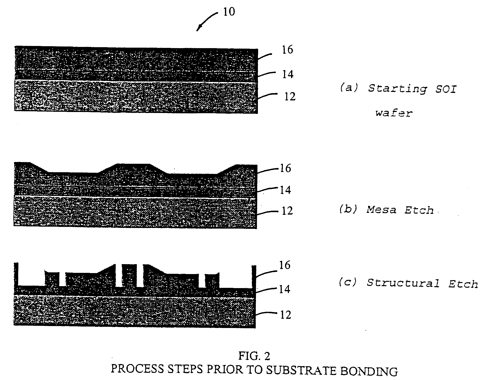
The invention provides a general fabrication method for producing MicroElectroMechanical Systems (MEMS) and related devices using Silicon-On-Insulator (SOI) wafer. The method includes providing an SOI wafer that has (i) a handle layer, (ii) a dielectric layer, and (iii) a device layer, wherein a mesa etch has been made on the device layer of the SOI wafer, providing a substrate, wherein a pattern has been etched onto the substrate, bonding the SOI wafer and the substrate together, removing the handle layer of the SOI wafer, removing the dielectric layer of the SOI wafer, then performing a structural etch on the device layer of the SOI wafer to define the device.

Description

CROSS-REFERENCE TO RELATED APPLICATIONS [0001] This application is a continuation in part of U.S. patent application Ser. No. 10 / 038,890, filed on Jan. 2, 2002, the disclosure of which is incorporated herein by reference. U.S. patent application Ser. No. 10 / 038, 890 claims priority to U.S. Provisional Patent Application Ser. No. 60 / 259,282, filed Jan. 2, 2001. The present application also claims priority of U.S. Provisional Patent Application Ser. No. 60 / 403,796, filed on Aug. 15, 2002.FIELD OF THE INVENTION [0002] The invention relates generally to MicroElectroMechanical Systems (MEMS), in particular, to methods for microfabricating MEMS devices on Silicon-On-Insulator (SOI) wafers. BACKGROUND OF THE INVENTION [0003] The rapidly emerging field of MicroElectroMechanical Systems (MEMS) has penetrated a wide array of applications, in areas as diverse as automotives, inertial guidance and navigation, microoptics, chemical and biological sensing, and biomedical engineering. Use of Silic...

Claims


Application Information

Patent Timeline
Patent Type & Authority Applications(United States)
IPC IPC(8): H01L21/76B81C1/00B81C3/00H01LH01L21/00H01L29/06
CPCB81C1/00182B81C2201/0191B81C3/001B81C1/00579
Inventor SAWYER, WILLIAM D.BORENSTEIN, JEFFREY T.
Owner CHARLES STARK DRAPER LABORATORY
Learn More