
Method for fabricating electrical connection structure of circuit board

a technology of electrical connection and circuit board, which is applied in the direction of manufacturing tools, printing element electric connection formation, and so on, can solve the problems of reducing fabrication reliability, unable to reduce stencil fabrication cost, and difficulty in allowing solder material to pass through the opening, so as to reduce fabrication reliability, eliminate fabrication bottlenecks, and reduce stencil fabrication cost

Active Publication Date: 2006-01-05
PHOENIX PRECISION TECH CORP
View PDF2 Cites 21 Cited by
  • Summary
  • Abstract
  • Description
  • Claims
  • Application Information

AI Technical Summary

Benefits of technology

The present invention provides a method for fabricating an electrical connection structure of a circuit board that overcomes the difficulties and drawbacks of prior-art stencil printing technology. The method allows for the formation of conductive structures such as plated through holes, conductive vias, and conductive circuits within the circuit board, and the attachment of a conductive base for electrically connecting the pads on the surface of the circuit board. The method also eliminates the need for complex procedures and high costs associated with the formation of solder material on the pad using an electroplating process. Additionally, the method solves the reliability problem caused by the contamination of the pad, conductive layer, and fabricated solder material. Overall, the method provides a cost-effective and reliable solution for fabricating electrical connection structures of circuit boards.

Problems solved by technology

Thus, a cost of stencil fabrication cannot be reduced due to difficulties in performing mold opening of the stencil.
Also, it is of difficulties to allow the solder material to pass through the opening due to smallness of the opening.
Therefore, the stencil has to be wiped out after performing a certain number of printings to ensure the cleanness of the stencil during practical operation, otherwise the shape and dimension of the solder material might be altered to cause an inconvenience as well as a decreased reliability in fabrication.
Although the foregoing method is able to eliminate drawbacks in the prior-art stencil printing technology, the procedures are very complex and the cost is very high.
Also, when the solder material is formed on the pad using the electroplating process, the thin metal layer serving as the current conductive path might be affected by the electroplating resist layer located above the conductive layer, therefore contaminating the pad, the conductive layer and the fabricated solder material.
Additionally, in order to form sufficient solder materials on the pad using the electroplating process, the criteria on the characteristics and thickness of the electroplating resist layer is very stringent, such that the fabrication is complicated as a consequence.
Finally, during the subsequent removal of the electroplating resist layer, the fabricated solder material formed in the electroplating resist layer might be influenced to cause a reliability problem.

Method used


Image

  • Method for fabricating electrical connection structure of circuit board
  • Method for fabricating electrical connection structure of circuit board
  • Method for fabricating electrical connection structure of circuit board

Examples


Embodiment Construction

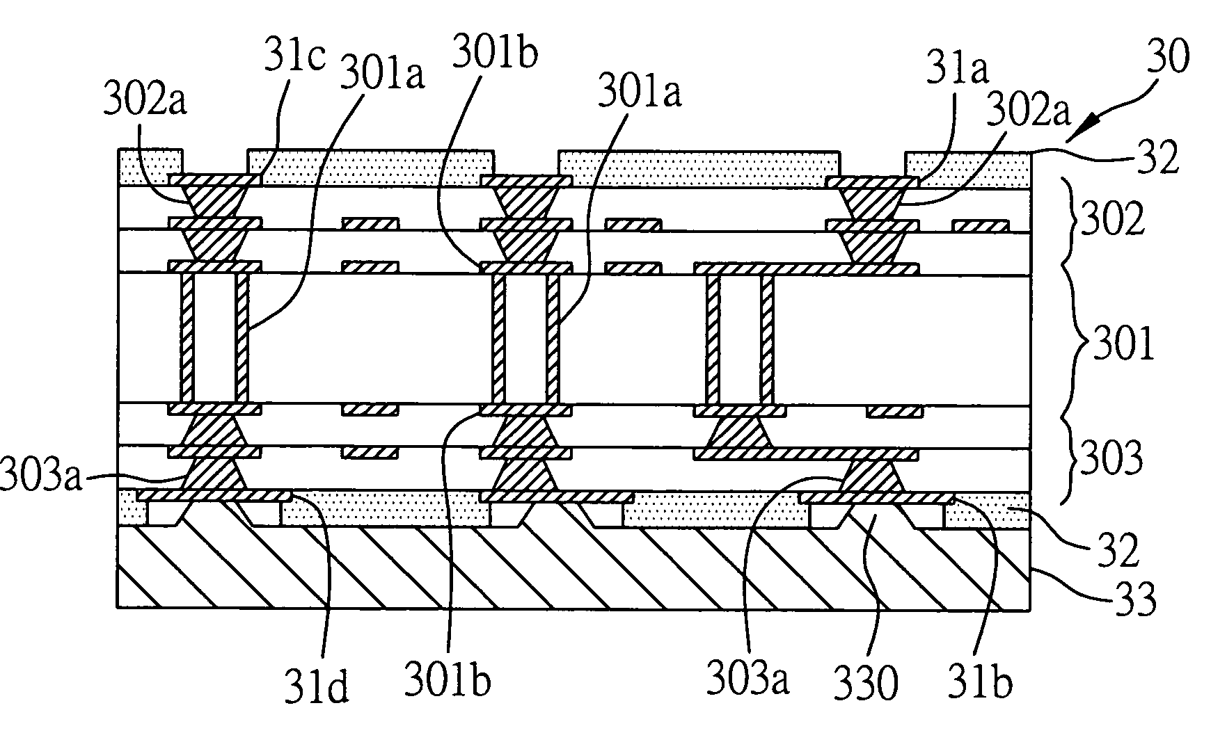
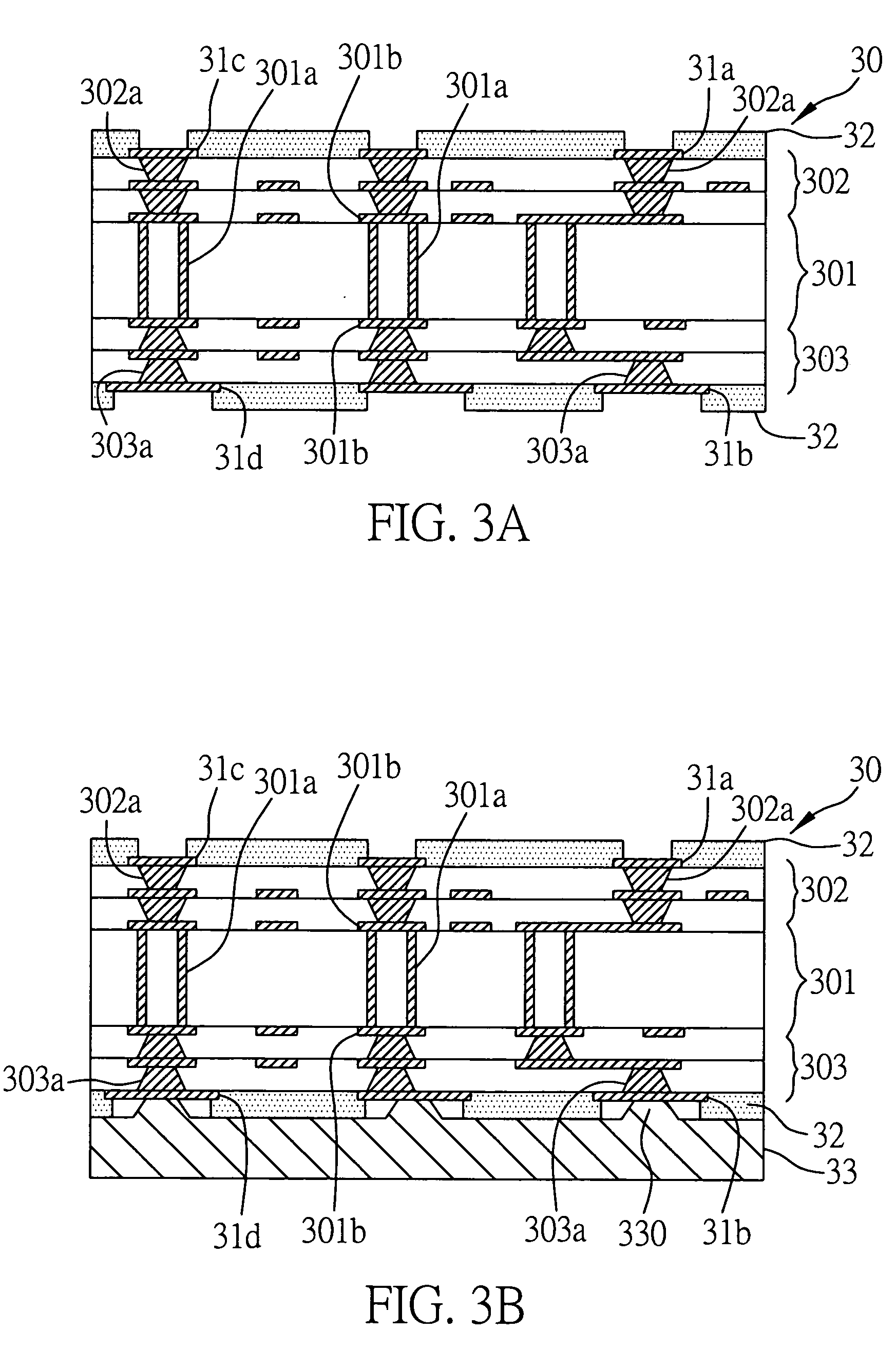
[0024]FIGS. 3A to 3D are cross-sectional views of a method for fabricating an electrical connection structure of a circuit board according to the first embodiment of the present invention.

[0025] Referring to FIG. 3A, a circuit board 30 having an internal circuit being completely electrically connected is provided. The circuit board 30 comprises a core circuit board 301 and a plurality of build-up circuit structures 302 and 303 formed on top and bottom surfaces of the core circuit board 301. Also, a plurality of pads 31a and 31b are formed on top and bottom surfaces of the circuit board 30. A plated through hole 301a formed penetrating through the core circuit board 301 is used for electrically connecting circuits 301b located on the top and bottom surfaces of the core circuit board 301. Similarly, a plurality of conductive vias 302a and 303a are used for electrically interconnecting the build-up circuit structures 302 and 303 respectively located on the top and bottom surfaces of t...


PUM

PropertyMeasurementUnit
conductiveaaaaaaaaaa
electrically active areaaaaaaaaaaa
electrically inactiveaaaaaaaaaa

Abstract

A method for fabricating an electrical connection structure of a circuit board is proposed. The circuit board is provided with a plurality of pads on a surface thereof and with a plurality of conductive structures therein for electrically connecting the pad. A plurality of openings is formed penetrating through an insulating layer provided on the circuit board to expose the pad. Subsequently, a conductive base is attached to one surface of the circuit board for electrically connecting the pad. By such arrangement, a conductive material can be formed on the pad located on the other surface of the circuit board by an electroplating process via the conductive base, the pad on the surface, and the conductive structure within the circuit board.

Description

FIELD OF THE INVENTION [0001] The present invention relates to a method for fabricating an electrical connection structure of a circuit board, and more particularly, to a method for fabricating an electrical connection structure which provides electrical conduction between the circuit board and electrical elements. BACKGROUND OF THE INVENTION [0002] Referring to the current flip-chip technique, electrode pads are located on a surface of a semiconductor integrated circuit (IC) chip and a corresponding pad is provided on an organic circuit board. Solder bumps or other conductively adhesive materials are mounted on an active surface of the chip, which is provided on the top of the circuit board, such that the solder bump or other conductively adhesive material can be used as input / output connections for electrically and mechanically connecting the chip to the circuit board. [0003] Referring to FIG. 1 which demonstrates a flip chip element known in the prior-art, a plurality of metal bu...

Claims


Application Information

Patent Timeline
Patent Type & Authority Applications(United States)
IPC IPC(8): B23K31/02B23K3/06H05K3/24H05K3/28H05K3/32H05K3/34H05K3/40H05K3/46
CPCB23K3/0623Y10T29/49126H05K3/242H05K3/28H05K3/3473H05K3/4007H05K3/4602H05K2201/0367H05K2201/09054H05K2201/09481H05K2203/0152H05K2203/043H05K2203/1581Y10T29/49165Y10T29/49147Y10T29/49155Y10T29/49167B23K2201/42B23K2101/42
Inventor WANG, YING-TUNG
Owner PHOENIX PRECISION TECH CORP
Learn More