Semiconductor laser and method for manufacturing the same

a semiconductor laser and laser technology, applied in semiconductor lasers, semiconductor/solid-state device details, lasers, etc., can solve the problems of reducing the band gap of the resonator end face, affecting the performance of the laser, so as to achieve excellent heat resistance. the effect of

Inactive Publication Date: 2005-12-29
PANASONIC SEMICON SOLUTIONS CO LTD
View PDF13 Cites 3 Cited by
  • Summary
  • Abstract
  • Description
  • Claims
  • Application Information

AI Technical Summary

Benefits of technology

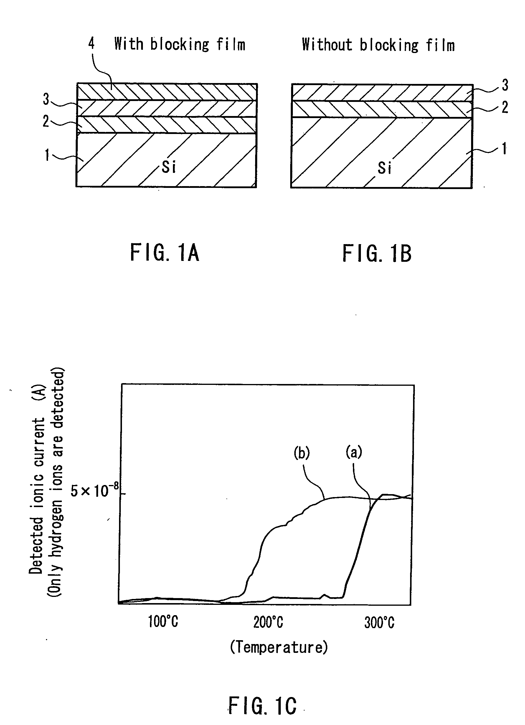
[0018] Therefore, with the foregoing in mind, it is an object of the present invention to provide a semiconductor laser having a hydrogen-added film in its end face coating films with excellent heat resistant properties and a method for manufacturing the same, by which when the semiconductor laser is exposed to high temperatures, the desorbed hydrogen in the end face coating film can be blocked, so that peeling of the end face coating film and deterioration of the end face coating film can be suppressed.

Problems solved by technology

In addition, heat is generated also due to the light absorption by the end face coating film itself, resulting in a decrease in the band gap of the resonator end face.
As a result of such a positive feedback involving the light absorption and the heat generation, finally COD occurs so that the resonator end face of the semiconductor laser melts, resulting in the breakage of a mirror of the resonator.
Then, a threshold current increases and optical output properties deteriorate considerably, so that a predetermined high output power cannot be obtained.
Especially since an absorption coefficient of a semiconductor laser with a shorter emission wavelength tends to increase, GaInP / AlGaInP based semiconductor lasers with an emission wavelength of 630 to 680 nm are susceptible to such tendency, which hinders the realization of high output power for such semiconductor lasers.
Thus, a distortion due to the residual stress causes deterioration in laser properties and reliability during a long term operation.
If the peeling of the end face coating film occurs, the laser outgoing end face is exposed to the air, and therefore this face is oxidized during a long term operation, which leads to the deterioration of the resonator end face and degrades the reliability.
Furthermore, the hydrogen-added amorphous silicon film, although intended to decrease the absorption coefficient, causes the following problems: that is, the desorption of hydrogen due to the application of heat causes a change in the refractive index of the film, resulting in an increase in the absorption coefficient as well as a change in the end face reflectance, which degrades the generation level of COD and the laser properties.

Method used


Image

  • Semiconductor laser and method for manufacturing the same
  • Semiconductor laser and method for manufacturing the same
  • Semiconductor laser and method for manufacturing the same

Examples


embodiment 1

[0045]FIG. 2 shows a semiconductor laser 101 according to Embodiment 1 of the present invention. Reference numeral 101a denotes an active layer. At a resonator end face 102 on the side of mainly emitting a laser beam from the semiconductor laser 101, a low-reflection film 103 is formed as an end face coating film, whereas at a resonator end face 104 on the other side, a high-reflection film 105 is formed as an end face coating film.

[0046] The low-reflection film 103 may be made up of a silicon oxide film formed directly on the resonator end face 102, and a film thickness of the low-reflection film 103 is designed so that the end face reflectance becomes about 5%.

[0047] The high-reflection film 105 may be made up of six layers including two sets of a silicon oxide film 107 formed directly on the resonator end face 104, a silicon nitride film 108 formed on the silicon oxide film 107 and a hydrogen-added amorphous silicon film 109 formed on the silicon nitride film 108. A film thickn...

embodiment 2

[0071]FIG. 6 shows a semiconductor laser 401 according to Embodiment 2 of the present invention. Reference numeral 401a denotes an active layer. This semiconductor laser 401 is different from the semiconductor laser 101 of Embodiment 1 in that a high-reflection film 405 on the side of a resonator end face 404 is made up of eight layers including a first silicon oxide film 107 formed directly on the resonator end face of the semiconductor laser 401, and a first silicon nitride film 108, a first hydrogen-added amorphous silicon film 109, a second silicon nitride film 108, a second silicon oxide film 107, a third silicon nitride film 108, a second hydrogen-added amorphous silicon film 109 and a fourth silicon nitride film 108, which are laminated successively on the first silicon oxide film 107. A low-reflection film 403 on the side of a resonator end face 402 is the same as in Embodiment 1.

[0072] One of the features of this embodiment resides in that the silicon nitride films 108 are...

embodiment 3

[0080]FIG. 8 shows a semiconductor laser according to Embodiment 3 of the present invention. This semiconductor laser has a configuration in which two semiconductor laser elements 502 and 503 are formed monolithically on the same substrate 501. Reference numeral 502a denotes an active layer of the semiconductor laser element 502. The semiconductor laser elements 502 and 503 may be configured so as to emit laser beams with different emission wavelengths from each other.

[0081] With respect to the resonator end faces of the semiconductor laser with such a configuration also, the end face coating film is applicable in the same manner as in the above-described embodiments. FIG. 8 shows a state in which the same low-reflection film 103 and the high-reflection film 105 as in FIG. 1 are formed.

[0082] In FIG. 8, the low-reflection film 103 and the high-reflection film 105 are formed as films common to the semiconductor laser elements 502 and 503. This is because a considerably minute space...


PUM


Abstract

A semiconductor laser includes an active layer formed on a substrate and a pair of cladding layers sandwiching the active layer. On at least one of resonator end faces of the semiconductor laser, a first dielectric film with hydrogen added therein is provided. Between the first dielectric film and the resonator end face, a second dielectric film for suppressing the diffusion of hydrogen is provided. Even when a semiconductor laser with an end face coating film including a hydrogen-added film is exposed to high temperatures, peeling of the end face coating film and deterioration of the end face coating film can be suppressed.

Description

[0001] This application is a division of application Ser. No. 10 / 368,206, filed Feb. 18, 2003, which is incorporated herein by reference.BACKGROUND OF THE INVENTION [0002] 1. Field of the Invention [0003] The present invention relates to a semiconductor laser and a method for manufacturing the same. More particularly, the present invention relates to a method for manufacturing a semiconductor laser with excellent heat resistant properties to avoid the deterioration in qualities of a coating film provided at an end face thereof under high temperature conditions, so that a level of Catastrophic Optical Damage (hereinafter abbreviated as COD) can be reduced and reliability can be improved. [0004] 2. Related Background Art [0005] In recent years, recording and reproducing type optical disk devices such as DVD-RAM and CD-R are in increasing demand. GaInP / AlGaInP based semiconductor lasers (emission wavelength: 630 to 680 nm) and AlGaAs based semiconductor lasers (emission wavelength: 780...

Claims


Application Information

Patent Timeline
Patent Type & Authority Applications(United States)
IPC IPC(8): H01S5/028
CPCH01S5/028
Inventor UEDA, TETSUOYAMANE, KEIJIKIDOGUCHI, ISAOFUJIMORI, SHOJI
Owner PANASONIC SEMICON SOLUTIONS CO LTD
Why Eureka
Try Eureka