Semiconductor device, electronic apparatus, and access control method of the semiconductor device

a technology of semiconductor devices and access control methods, applied in the direction of unauthorized memory use protection, instruments, error detection/correction, etc., can solve the problems of complicated communication control with external devices, higher cost of developing environment, and problematically complicating the configuration and control of semiconductor devices. , to achieve the effect of simple configuration

Inactive Publication Date: 2005-12-01
SEIKO EPSON CORP
View PDF4 Cites 29 Cited by
  • Summary
  • Abstract
  • Description
  • Claims
  • Application Information

AI Technical Summary

Benefits of technology

[0010] According to the present invention, since the debug-enable signal input terminal is provided, whether or not a general purpose debugger is connected thereto can be detected without providing any additional circuits to the debugger or the like. Further, it is arranged that the debugging function is enabled by the debug-enable signal, and in the enabled state, the access signal from the debugger to the semiconductor device is validated, further, the security circuit detects connection of the debugger to temporally disable access to the main memory. After then, if input data expressed by at least a part of the access signal is predetermined data, the security circuit enables the debugger to access the main memory Thus, since a general purpose debugger can be used, and illegal access to the memory from the general purpose debugger can be restricted with a simple configuration, system development cost can be reduced.
[0025] According to the present invention, an electronic apparatus including a semiconductor device capable of being developed with a general purpose debugger, and preventing reverse engineering in which the data in the main memory is analyzed by illegal access from the debugger, and surely protecting licensed highly confidential information can be provided.

Problems solved by technology

The technology disclosed in Japanese Unexamined Patent Publication No. 2003-177938, however, which requires an additional external device, incurs a higher cost of the developing environment.
Further, since software for realizing security functions must be implemented in the semiconductor device, the communication control with external devices is made complicated.
Moreover, an additional security measure is required such as separately storing data for realizing the security function and data to be kept strictly confidential in the semiconductor device, which problematically complicates the configuration and control of the semiconductor device.

Method used


Image

  • Semiconductor device, electronic apparatus, and access control method of the semiconductor device
  • Semiconductor device, electronic apparatus, and access control method of the semiconductor device
  • Semiconductor device, electronic apparatus, and access control method of the semiconductor device

Examples


Embodiment Construction

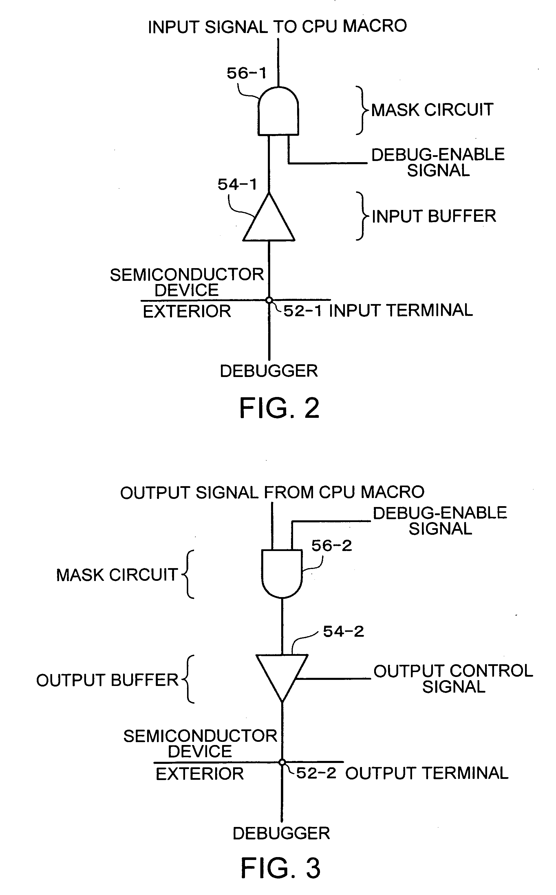
[0045] Hereinafter, an embodiment of the present invention is described in detail with reference to the accompanying drawings. Note that the embodiment described below does not unreasonably limit the content of the present invention as claimed in the claim section. Further, it is not necessary that all components of the configuration described below are essential elements of the present invention.

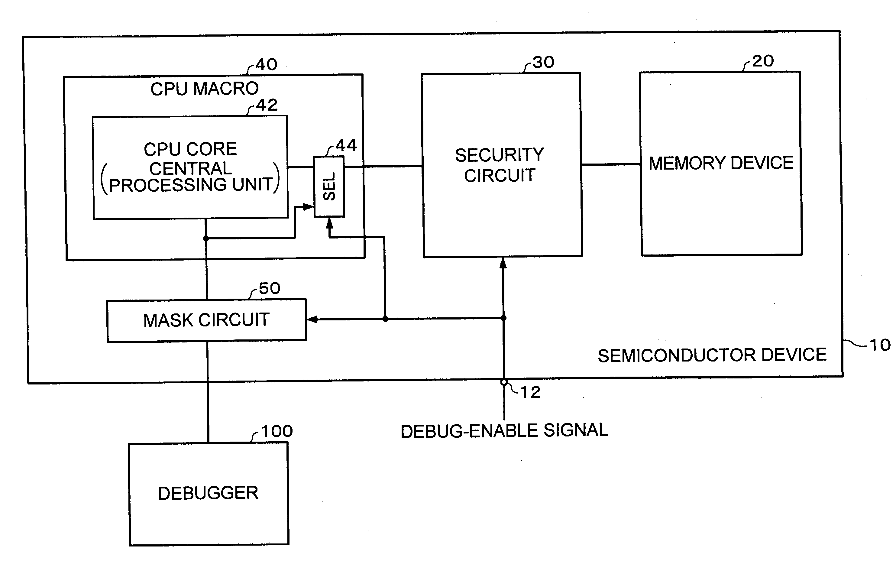
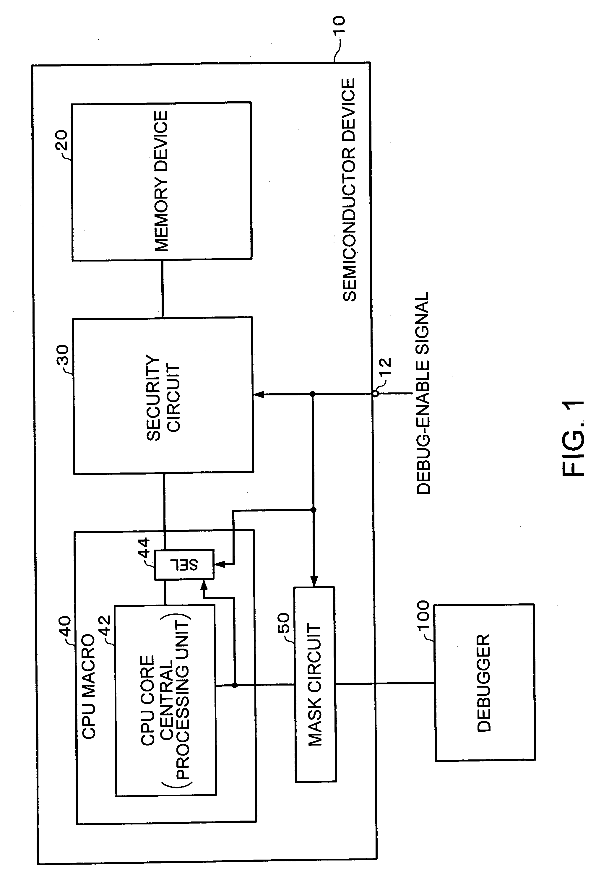
[0046]FIG. 1 shows a block diagram of a principle configuration of the semiconductor device according to the present embodiment.

[0047] The semiconductor device 10 (IC, semiconductor circuit, semiconductor integrated circuit) includes a memory device 20 and a security circuit 30. The memory device 20 stores the access data of the CPU (central processing unit). The memory device 20 can be called as a main memory. The security circuit 30 restricts access of the CPU or a debugger 100 to the memory device 20. The debugger 100 having an emulation function of the CPU accesses the memory device 2...


PUM


Abstract

The semiconductor device comprises a memory for storing access data of a central processing unit, a security circuit for restricting access to the memory from one of the central processing unit and a debugger having an emulation function of the central processing unit and for accessing the memory as a substitute of the central processing unit, and a debug-enable signal input terminal. When the debug-enable signal is inactive, an access signal from the debugger to the semiconductor device is invalidated, and the security circuit enables the central processing unit to access the memory. When the debug-enable signal is active, the access signal becomes valid, and the security circuit disables access to the memory. After then, when a password for access is input from the debugger, the security circuit enables the debugger to access the memory.

Description

RELATED APPLICATIONS [0001] This application claims priority to Japanese Patent Application No. 2004-125735 filed Apr. 21, 2004 which is hereby expressly incorporated by reference herein in its entirety. BACKGROUND [0002] 1. Technical Field [0003] The present invention relates to a semiconductor device, an electronic apparatus, and an access method of the semiconductor device. [0004] 2. Related Art [0005] In some cases, data necessary to be kept strictly confidential may be stored in a memory implemented in a semiconductor device. In particular, in a semiconductor device equipped with a central processing unit (CPU) and a memory storing source codes which are access data of the CPU, the data necessary to be kept strictly confidential may sometimes be included in the source codes. In such a case, it is necessary to prevent illegally accessing the memory by a debugger used to develop a system using the semiconductor device. Therefore, some security measures must be taken considering t...

Claims


Application Information

Patent Timeline
IPC IPC(8): G06F11/00G06F12/14G06F21/60G06F21/62G06F21/75
CPCG06F21/79G06F11/3648
Inventor KUMAGAI, TOMONORI
Owner SEIKO EPSON CORP
Why Eureka
Try Eureka