Internal voltage generating circuit and semiconductor integrated circuit device

Active Publication Date: 2005-12-01
RENESAS ELECTRONICS CORP
View PDF14 Cites 35 Cited by
  • Summary
  • Abstract
  • Description
  • Claims
  • Application Information

AI Technical Summary

Benefits of technology

[0014] Accordingly, an object of the invention is to provide an internal voltage generating circuit, which can easily adjust temperature characteristics, and thereby can generate a precise reference voltage.
[0015] Another object of the invention is to provide an internal voltage generating circuit, which can produce an internal voltage with low current consumption even in a fast operation by utilizing the above reference voltage.
[0016] Still another object of the invention is to provide a semiconductor integrated circuit device provided with a power supply circuit, which can produce an internal voltage with low current consumption even in a system LSI.
[0017] Yet another object of the invention is to provide a semiconductor integrated circuit device, which can stably supply an internal voltage to a plurality of core circuits with low power consumption even under conditions of low power supply voltage.
[0020] In the internal voltage generating circuit according to the first aspect of the invention, the voltage-follower-connected differential amplifier circuit receives the first reference voltage, and the second reference voltage is produced by dividing the output voltage of the differential amplifier circuit. The second reference voltage is set as a target voltage level. Therefore, the first reference voltage can be set to a voltage level higher than a desired voltage level, and temperature characteristics of the first reference voltage can be controlled even with a low power supply voltage so that it is possible to produce the reference voltage at the desired voltage level, of which temperature characteristics are adjusted precisely. Also, the internal voltage at a predetermined voltage level can be precisely produced based on the reference voltage thus produced.
[0021] In a semiconductor integrated circuit device according to the second aspect of the invention, the standby module is arranged commonly to the plurality of core circuits, and the time required for conducting tests on the current consumption and standby current in the standby mode can be reduced as compared with a structure arranging an independent standby module for each core circuit. It is not necessary to arrange the independent standby module for each core circuit so that an area occupied by the core circuits can be small.

Problems solved by technology

Among various uses, mobile communication terminal devices, movie processing and communication networks strongly require such system LSIs, and these uses require high operation frequencies and low power consumption.
Therefore, it is required only to increase operation speeds of column-related circuits, which are provided in connection with selection of the memory cell column, and current consumption is relatively small even in a fast operation.
However, if the power supply voltage is lowered for reducing the power consumption, these reference voltage generating circuit and constant current generating circuit operate in circuit operation regions close to threshold voltages of transistors, and it becomes difficult to operate stably the MOS transistors and to adjust circuit operation characteristics.
Therefore, it becomes difficult to adjust sufficiently the temperature characteristics with a low power supply voltage.
However, no consideration is given to a manner of adjusting temperature characteristics of this reference voltage as well as a manner of stably producing the reference voltage with a low power supply voltage.

Method used


Image

  • Internal voltage generating circuit and semiconductor integrated circuit device
  • Internal voltage generating circuit and semiconductor integrated circuit device
  • Internal voltage generating circuit and semiconductor integrated circuit device

Examples


first embodiment

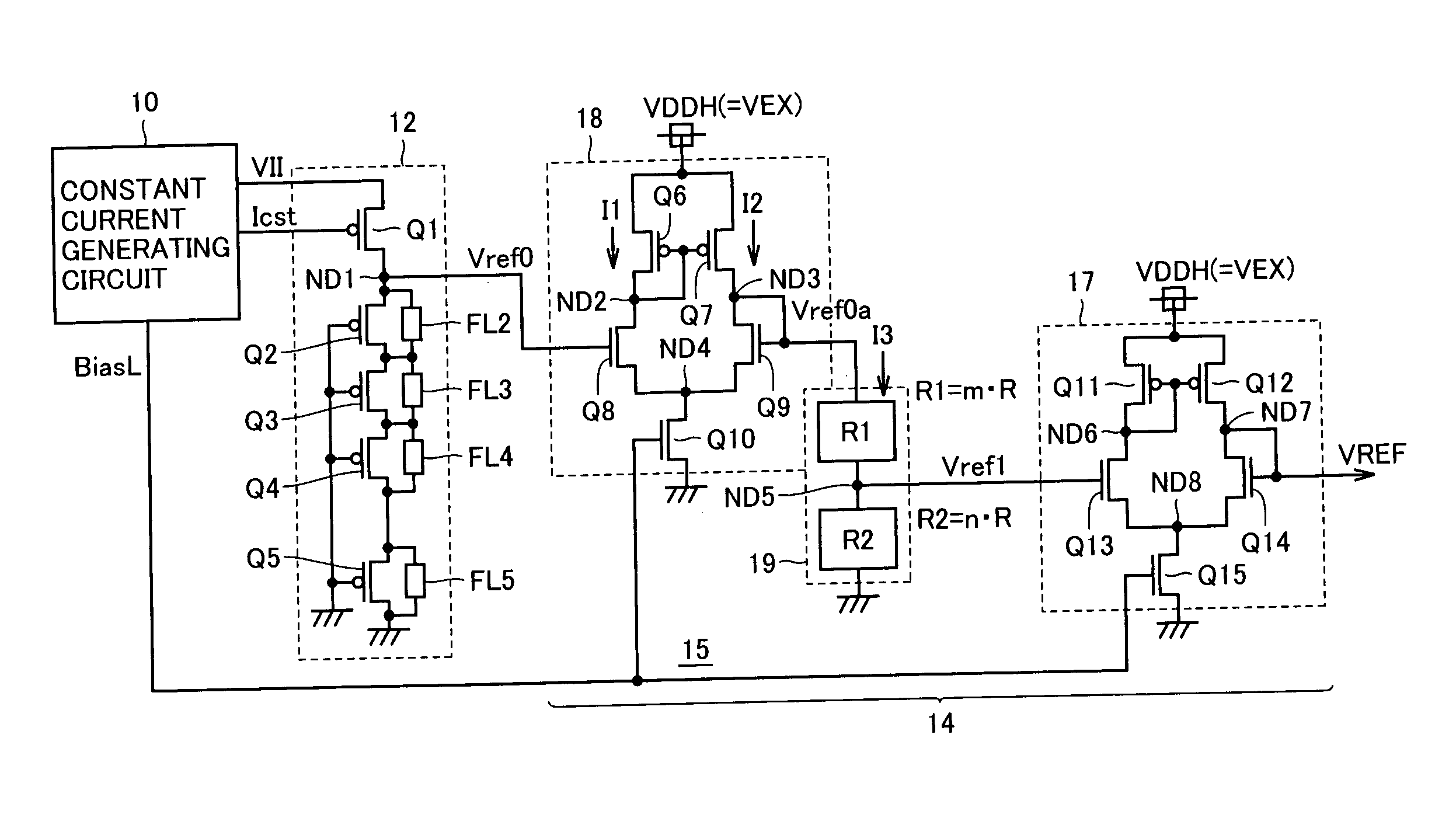
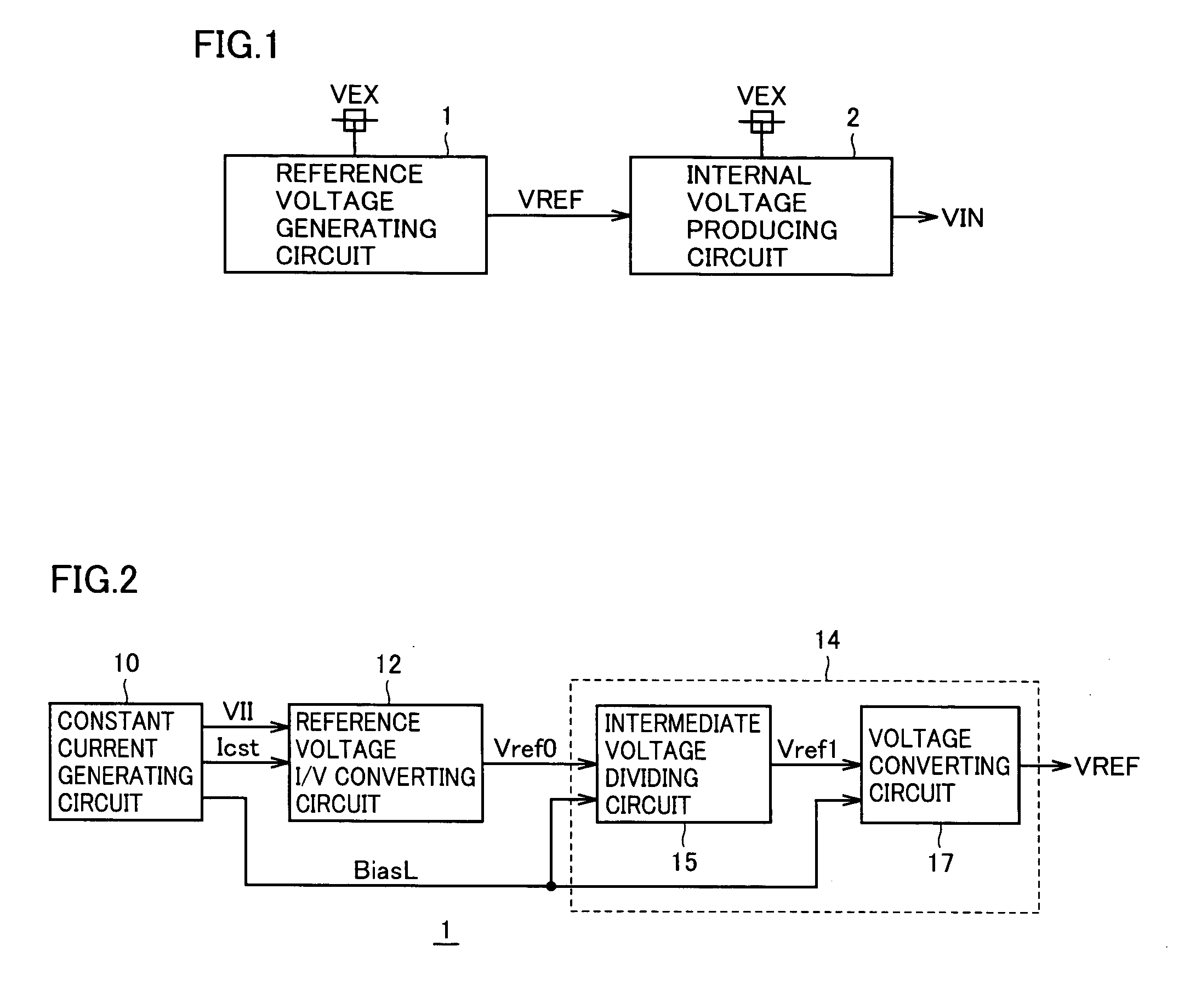
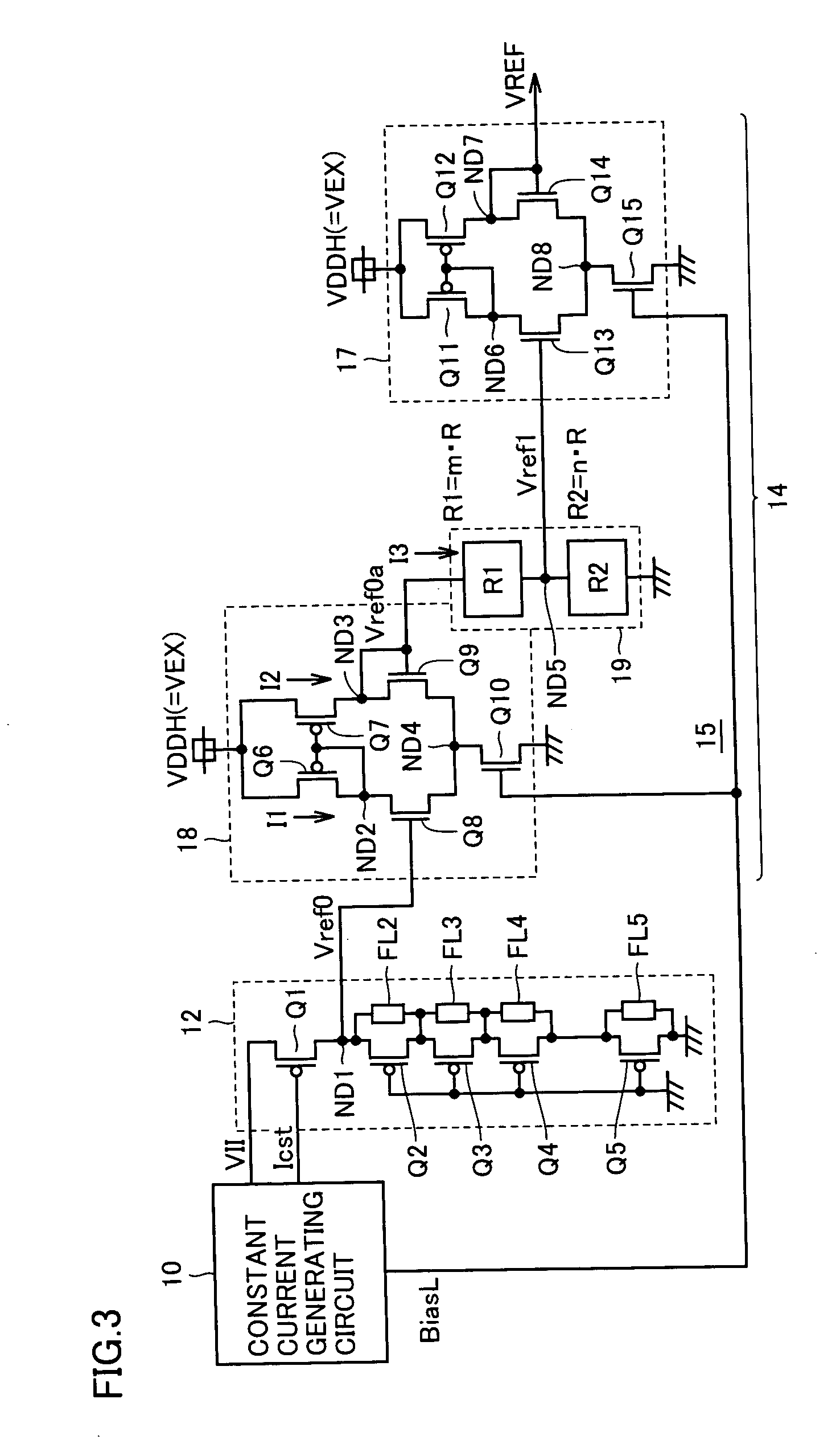
[0048]FIG. 1 schematically shows a structure of an internal voltage generating circuit according to the invention. In FIG. 1, the internal voltage generating circuit includes a reference voltage generating circuit 1 producing a reference voltage VREF, of which temperature characteristic is compensated, from an external power supply voltage VEX, and an internal voltage producing circuit 2, which produces an internal voltage VIN at a desired voltage level from external power supply voltage VEX by utilizing reference voltage VREF.

[0049] Reference voltage generating circuit 1 produces reference voltage VREF by performing resistance division on a first reference voltage higher than a target voltage level. The temperature compensation is effected on the first reference voltage, and thereby temperature characteristics of reference voltage VREF are adjusted.

[0050] A type of internal voltage VIN produced by internal voltage producing circuit 2 depends on a structure of a semiconductor devi...

second embodiment

[0078]FIG. 4 shows a structure of an internal voltage generating circuit according to a second embodiment of the invention. In FIG. 4, a circuit generating negative voltage VBB is shown as internal voltage producing circuit 2. If the corresponding core circuit is a DRAM, negative voltage VBB is applied to a substrate of a memory cell array. In the case of the negative voltage word line structure, negative voltage VBB is transmitted to an unselected word line or selected main word line (in the case of a hierarchical word line structure). In the case of a flash memory, negative voltage VBB is utilized in an erasing or writing operation.

[0079] In FIG. 4, internal voltage producing circuit 2 includes a detection level generating circuit 22 of a resistance division type effecting resistance division on reference voltage VREF provided from reference voltage generating circuit 1, a level detecting circuit 20 detecting a level of negative voltage VBB according to a divided voltage VrefB pr...

third embodiment

[0104]FIG. 9 schematically shows a structure of internal voltage producing circuit 2 according to a third embodiment of the invention. In FIG. 9, internal voltage producing circuit 2 includes a level detecting circuit 50 detecting a level of boosted voltage VPP based on reference voltage VREF provided from reference voltage generating circuit 1, an internal clock generating circuit 52, which is selectively activated according to an output signal of level detecting circuit 50, and thereby generates an internal clock signal of a predetermined period, and a booster pump circuit 54, which produces boosted voltage VPP by utilizing the charge pump operation of the capacitance element according to the internal clock signal provided from internal clock generating circuit 52.

[0105] Boosted voltage VPP is at a higher level than externally supplied power supply voltage VDDH (=VEX). The clock signal, which is produced by internal clock generating circuit 52 in the active state, has a high freq...


PUM


Abstract

A voltage for reference at a voltage level higher than a target value is produced from a constant current provided from a constant current generating circuit, and is subjected to resistance division by a resistance division circuit to produce a reference voltage at the target level, and then a final reference voltage is produced by a voltage follower. An internal voltage generating circuit thus provided can generate the reference voltage having the desired voltage level with high accuracy as well as an internal voltage based on the reference voltage by controlling temperature characteristic even with a low power supply voltage.

Description

BACKGROUND OF THE INVENTION [0001] 1. Field of the Invention [0002] The present invention relates to an internal voltage generating circuit and a semiconductor integrated circuit device using the same, and particularly to an internal voltage generating circuit, which can precisely produce an internal voltage stably having a desired temperature characteristic even with a low power supply voltage, and a semiconductor integrated circuit device, in which the internal voltage generating circuit can be arranged with high area utilizing efficiency for stable transmission of to various elements on a chip. [0003] 2. Description of the Background Art [0004] Owing to development of a semiconductor miniaturization technology in recent years, elements have been miniaturized to a higher extent, and high-density integration can now be achieved. The high-density integration has actualized an integrated circuit device, which includes a plurality of function circuits formed on a single chip to form o...

Claims


Application Information

Patent Timeline
IPC IPC(8): G05F1/10H01L27/04G05F1/46G05F3/24G11C11/407H01L21/822
CPCG05F1/465
Inventor GYOHTEN, TAKAYUKIMORISHITA, FUKASHI
Owner RENESAS ELECTRONICS CORP
Why Eureka
Try Eureka