
Determining leakage in matrix-structured electronic devices

Active Publication Date: 2005-11-24
DOLYA HOLDCO 5 LTD
View PDF6 Cites 13 Cited by
  • Summary
  • Abstract
  • Description
  • Claims
  • Application Information

AI Technical Summary

Problems solved by technology

Anode-cathode shorts within a pixel (“pixel shorts”) are one of the major causes for failure of passive matrix OLED devices.
The pixel short lowers the display quality and may even render the display unusable.
The pixel short can be caused by, for example, substrate imperfections or asperities, anode layer irregularities, non-uniformity of the one or more organic layers, and airborne particles introduced in the element structure during handling.
Pixels with risk of shorting usually have an increased reverse leakage current at zero operation hours.
It is difficult to detect this leakage current due to the noise added by the multitude of pixels that are in parallel to the pixel to be measured.
In case of OLED displays, the measurement of pixel related leakage becomes particularly important, since there is a high probability that leaky pixels will develop into pixel shorts.
It is difficult and time consuming to detect such a small leakage current in each pixel of a display that has thousands of pixels.

Method used


Image

  • Determining leakage in matrix-structured electronic devices
  • Determining leakage in matrix-structured electronic devices
  • Determining leakage in matrix-structured electronic devices

Examples


first embodiment

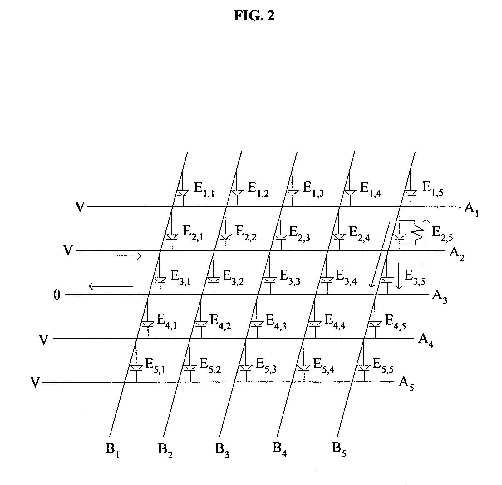
[0013] this invention pertains to a high throughput screening technique to identify current leakage in matrix-structured electronic devices. Because elements that are likely to develop a short have relatively high leakage current at zero operation hours, by identifying elements with the relatively high leakage current, the electronic devices that are more likely to later develop a short can be differentiated. The electronic devices can be, for example, passive matrix displays (e.g., OLED passive matrix displays where the active layers are comprised of organic polymers or small molecules; or inorganic LED passive matrix displays), light sources used for area illumination, active matrix displays, memory circuits, detector arrays, and solar cell arrays. The electronic device includes multiple elements (e.g., an EL element, a solar cell, or a photodetector cell), multiple first lines (e.g., cathode lines or anode lines), and multiple second lines (e.g., anode strips or cathode lines). T...

third embodiment

[0015] the present invention pertains to using optical detection by employing an array of infrared sensors to identify one or more leaky elements in the electronic device.

[0016] While the matrix-structured electronic device can be, for example, any of the devices described earlier, in order to provide concrete descriptions and examples, the descriptions and examples below refer to a passive matrix OLED display.

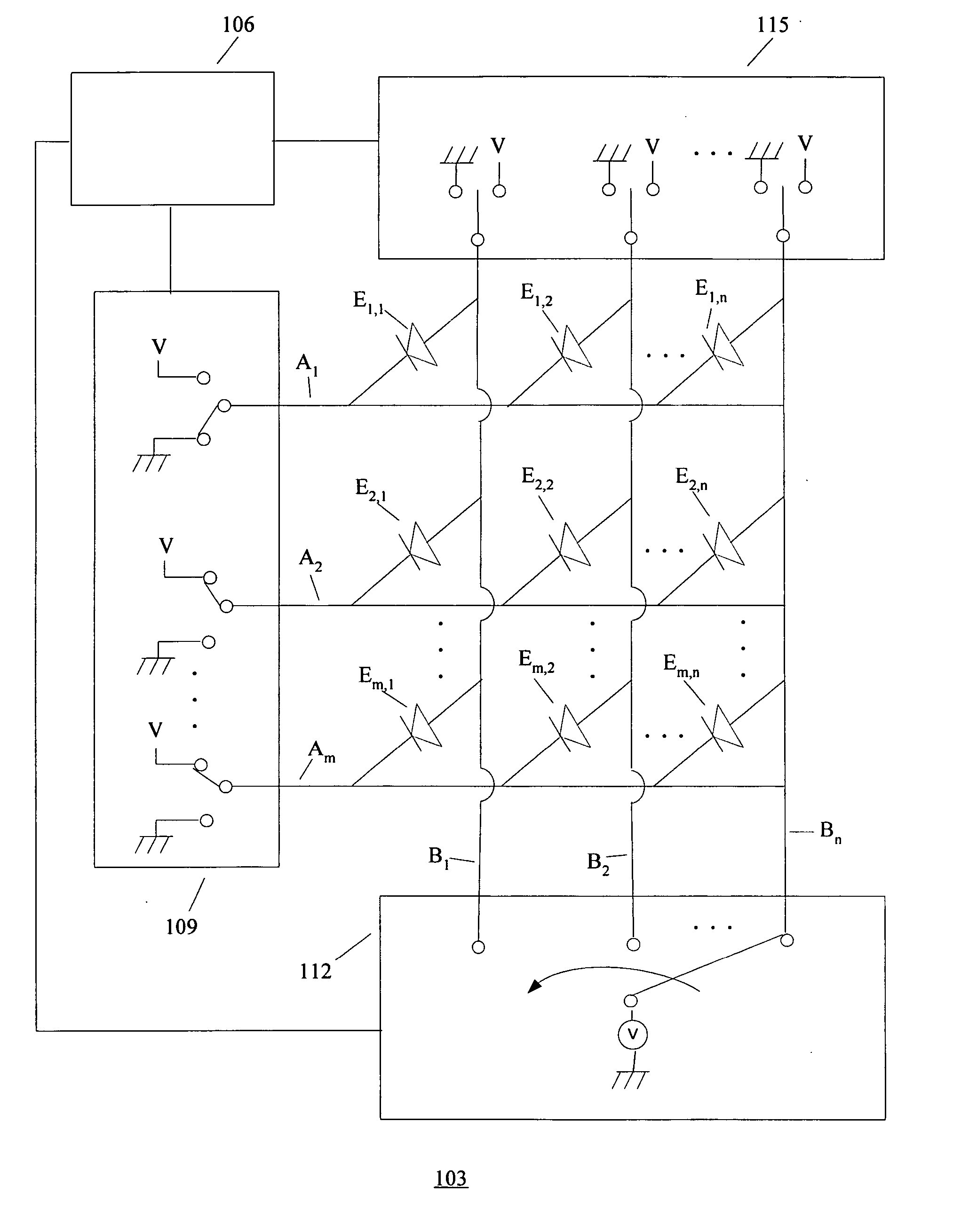
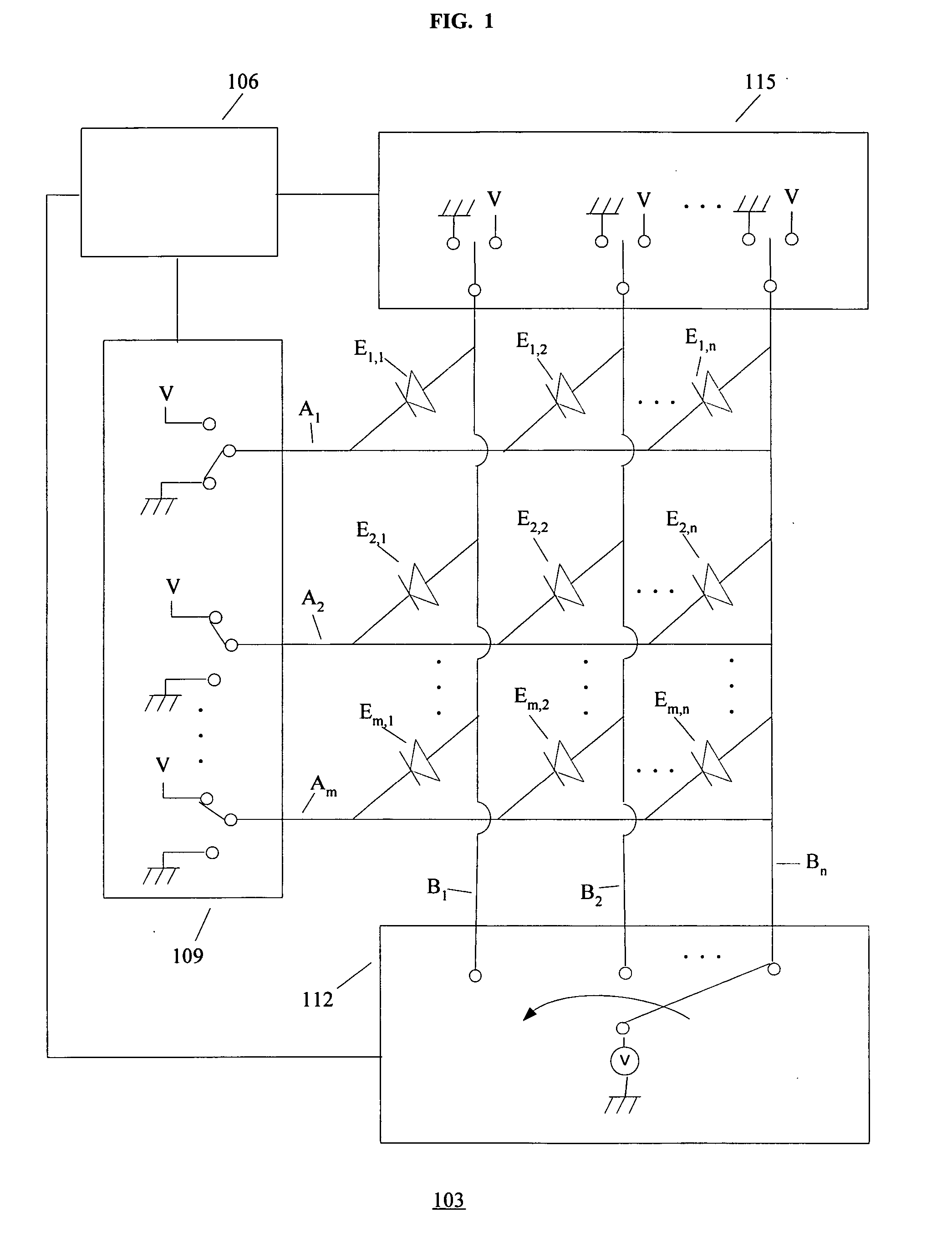
[0017]FIG. 1 shows an embodiment of a testing device 103 according to the present invention. The testing device 103 includes a control unit 106, a line drive unit 109, a line drive unit 115, and a voltage measuring device 112 (e.g., this device can include one voltmeter or multiple voltmeters). The control unit 106 is coupled to the line drive unit 109, the line drive unit 115, and the voltage measuring device 112. The line drive unit 109 is coupled to cathode lines A1 to Am (e.g., the cathode lines can be referred to generically as either the first lines or the second lines)...


PUM


Abstract

One embodiment of this invention pertains to a high throughput screening technique to identify current leakage in matrix-structured electronic devices. Because elements that are likely to develop a short have relatively high leakage current at zero operation hours, by identifying elements with the relatively high leakage current, the electronic devices that are more likely to later develop a short can be differentiated. The screening technique includes performing the following actions: selecting one of multiple first lines; applying a first voltage to the selected first line; applying a second voltage to the one or more of the first lines that are not selected; floating the multiple second lines; and measuring the voltages on the second lines, either sequentially one line at a time or measuring all the lines at the same time.

Description

CROSS-REFERENCE TO RELATED APPLICATIONS [0001] This application claims benefit of U.S. Provisional Patent Application having the Application No. 60 / 573,074 filed on May 21, 2004 and entitled “Determining Leakage in Matrix-Structured Electronic Devices.”BACKGROUND OF THE INVENTION [0002] An organic light emitting diode (“OLED”) display typically includes, in sequence: (1) a transparent anode (e.g., the anode can be comprised of indium tin oxide (“ITO”)); (2) a hole transporting layer (“HTL”); (3) an electron transporting and light emitting layer (“emissive layer”); and (4) a cathode. When a forward bias is applied, holes are injected from the anode into the HTL, and the electrons are injected from the cathode into the emissive layer. Both carriers are then transported towards the opposite electrode and allowed to recombine with each other in the device, the location of which is called the recombination zone; the recombinations in the emissive layer produce visible light. In an OLED d...

Claims


Application Information

Patent Timeline
IPC IPC(8): G01R31/00G01R31/30G09G3/00G09G3/32
CPCG01R31/3008G09G3/3216G09G3/006
Inventor SO, FRANKYPSCHENITZKA, FLORIANHOEFLING, EGBERT
Owner DOLYA HOLDCO 5 LTD
Learn More