
Composite layer method for minimizing PED effect

a composite layer and ped effect technology, applied in the field of photolithography processes, can solve problems such as adversely affecting the dimensions of device features, and achieve the effects of reducing the post-exposure delay (ped) effect, preventing or minimizing the q-time narrowing of the photo-cracked effect, and eliminating or preventing the ped

Inactive Publication Date: 2005-11-03
TAIWAN SEMICON MFG CO LTD
View PDF5 Cites 5 Cited by
  • Summary
  • Abstract
  • Description
  • Claims
  • Application Information

AI Technical Summary

Benefits of technology

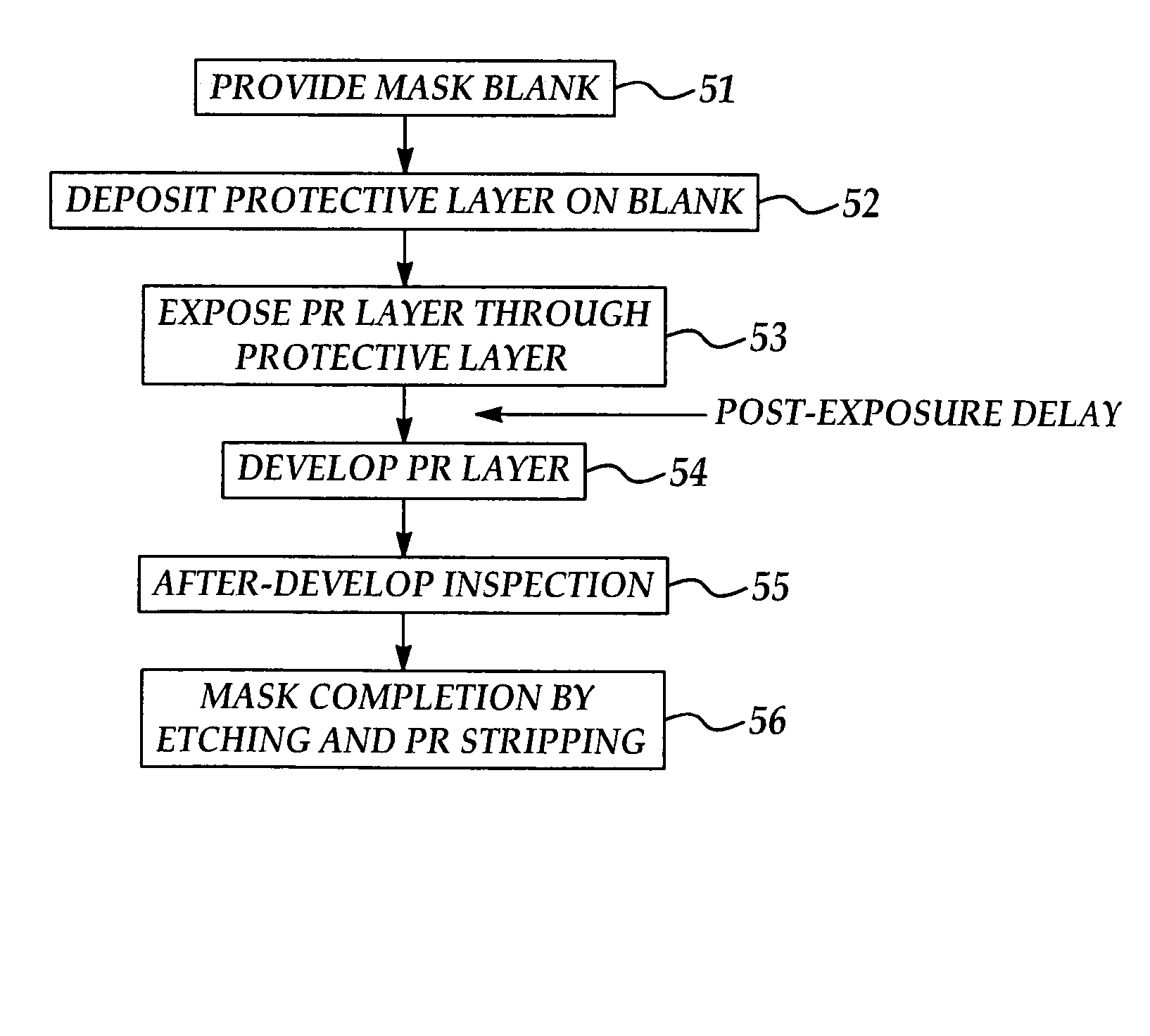
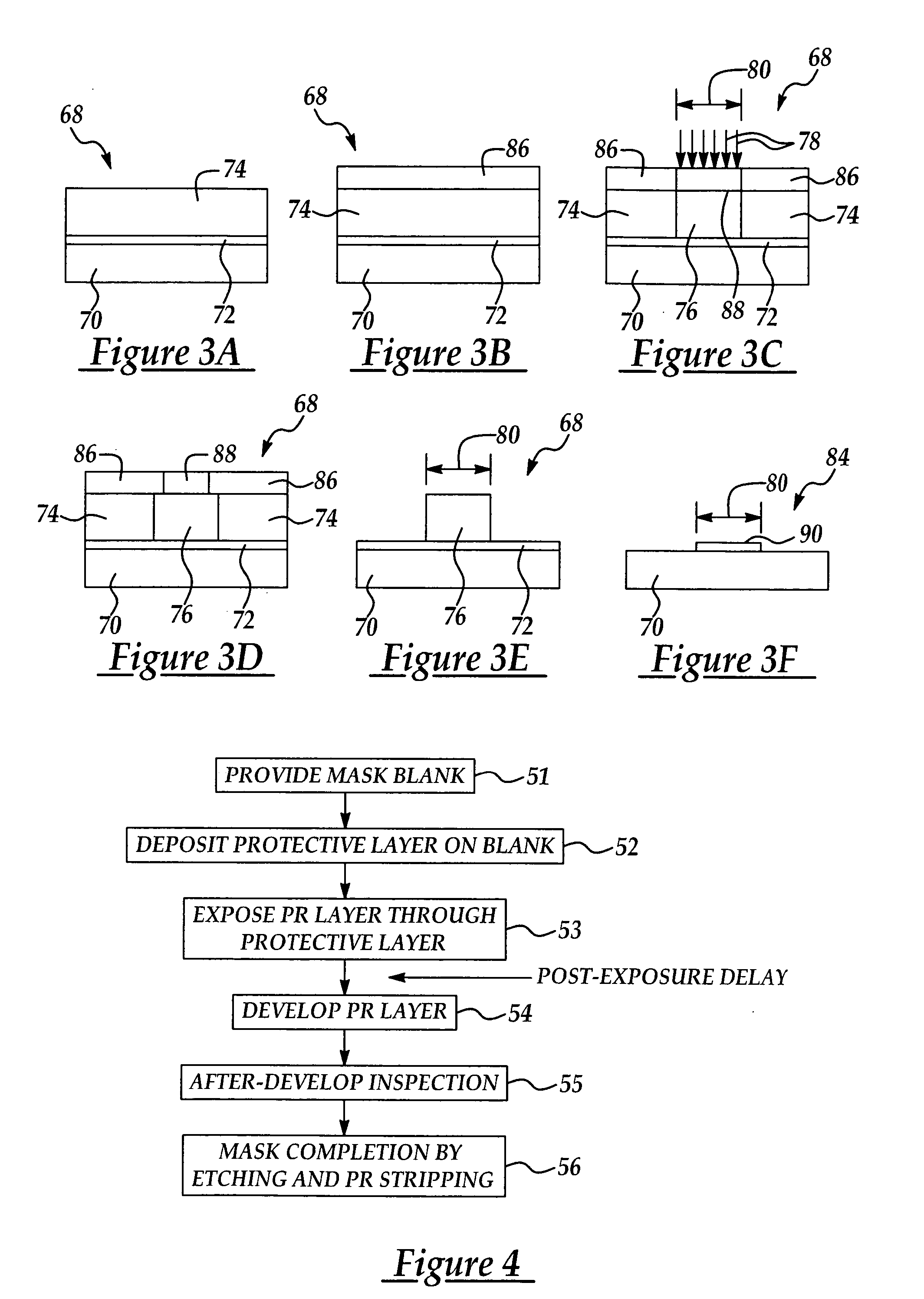
[0019] In accordance with these and other objects and advantages, the present invention is generally directed to a novel composite layer structure method which is suitable for reducing post-exposure delay (PED) effects associated with fabricating a photolithography reticle or mask and eliminating or at least minimizing variations between intended and realized critical dimension values for a circuit pattern fabricated on the reticle or mask. The method includes providing a mask blank having a metal layer, providing a photoresist layer on the metal layer of the mask blank, providing a protective layer on the photoresist layer and photo-cracking the photoresist layer in the desired circuit pattern typically by electron beam exposure. During subsequent post-exposure delay periods, the protective layer prevents or minimizes Q-time narrowing of the photo-cracked photoresist, and consequently, prevents or minimizes narrowing of the critical dimension of a circuit pattern etched in the metal layer according to the width of the photo-cracked photoresist.

Problems solved by technology

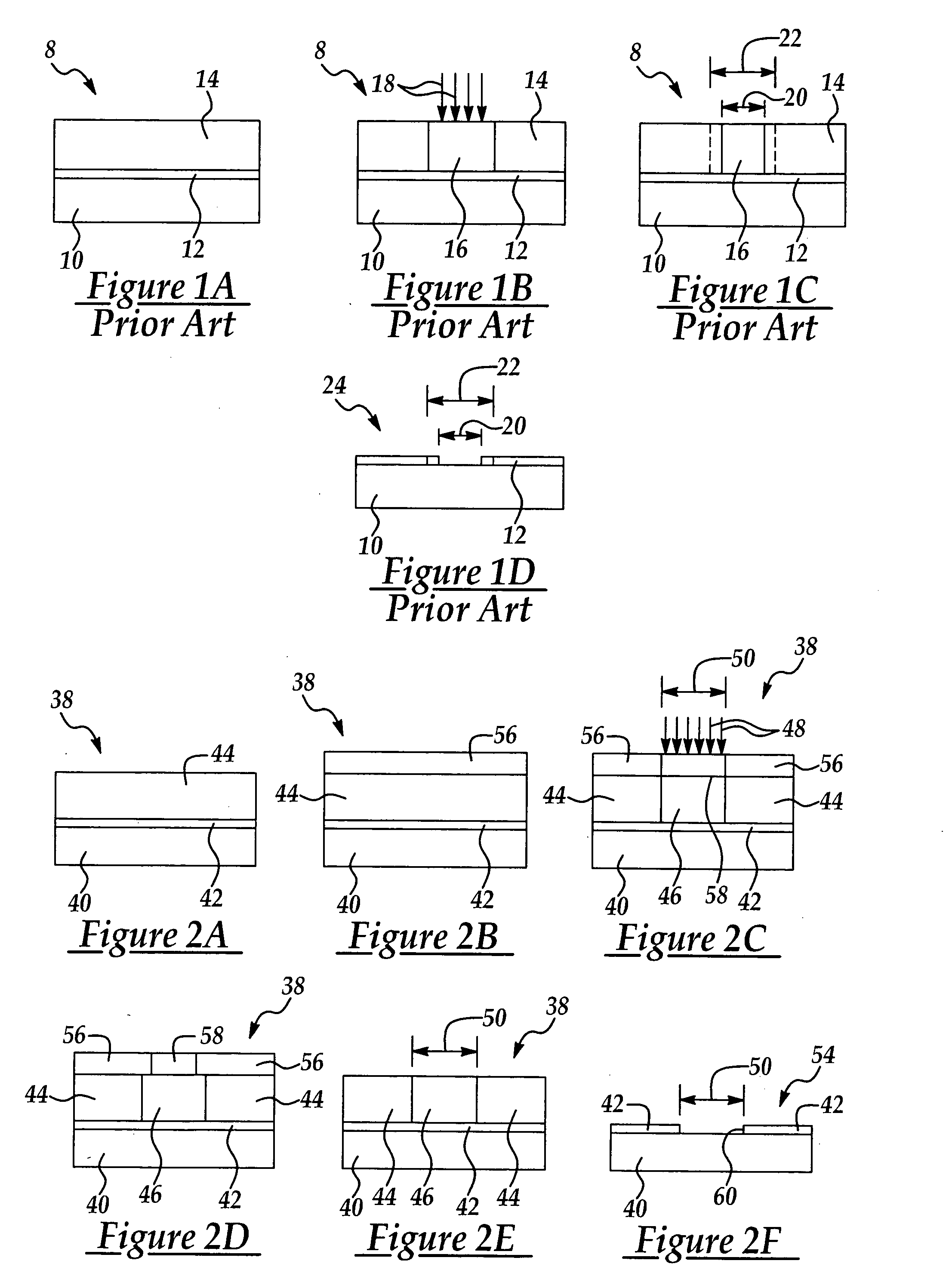
This adversely affects the dimensions of device features which are ultimately fabricated on the wafer based on the circuit pattern transferred to photoresist on the wafer using the fabricated mask 24.

Method used


Image

  • Composite layer method for minimizing PED effect
  • Composite layer method for minimizing PED effect
  • Composite layer method for minimizing PED effect

Examples


first embodiment

[0042] Referring to FIGS. 2A-2F, in the method according to the present invention, in a first step a mask blank 38 is obtained. The mask blank 38 includes a transparent substrate 40, such as quartz, and a typically metal blanket layer 42 such as chromium sputtered on the transparent substrate 40. The mask blank 38 may be conventional and is obtainable from the Hoya corp., for example. A layer of positive or negative photoresist 44, which may be multi-layered, is coated on the blanket layer 42. As shown in FIG. 2B, in a second step according to the method of the invention, a protective layer 56, which may be an organic positive or negative photoresist, is coated on the photoresist layer 44. The protective layer 56 may be a low-sensitivity negative-type chemical amplified resist (CAR) known by those skilled in the art. The mask blank 38 is then soft-baked at typically about 95 degrees C. for typically about 300 seconds to drive off solvent and harden the protective layer 56.

[0043] In ...

second embodiment

[0046] Referring next to FIGS. 3A-3F, in the method according to the present invention, as a first step a mask blank 68 is obtained. The mask blank 68 includes a blanket layer 72 such as chromium which is sputtered on a transparent substrate 70, such as quartz. A layer of positive or negative photoresist 74 is provided on the blanket layer 72 of the mask blank 68. As shown in FIG. 3B, in a second step according to the method of the invention, a protective layer 86, which may be an organic positive or negative photoresist, is deposited on the negative photoresist layer 74. The protective layer 86 is tyically a low-sensitivity negative-type chemical amplified resist (CAR) known by those skilled in the art. The mask blank 68 is then soft-baked at typically about 95 degrees C. for typically about 300 seconds to drive off solvent and harden the protective layer 86.

DESCRIPTION OF THE PREFERRED EMBODIMENTS

[0047] In a third step according to the method of the invention, shown in FIG. 3C, t...


PUM

PropertyMeasurementUnit
diameteraaaaaaaaaa
widthaaaaaaaaaa
widthaaaaaaaaaa

Abstract

A novel composite layer structure method which is suitable for reducing post-exposure delay (PED) effects associated with fabricating a photolithography reticle or mask and eliminating or at least minimizing variations between intended and realized critical dimension values for a circuit pattern fabricated on the reticle or mask. The method includes providing a mask blank having a metal layer, providing a photoresist layer on the metal layer of the mask blank, providing a protective layer on the photoresist layer and photo-cracking the photoresist layer in the desired circuit pattern typically by electron beam exposure. During subsequent post-exposure delay periods, the protective layer prevents or minimizes Q-time narrowing of the photo-cracked photoresist, and consequently, prevents or minimizes narrowing of the critical dimension of a circuit pattern etched in the metal layer according to the width of the photo-cracked photoresist.

Description

FIELD OF THE INVENTION [0001] The present invention relates to photolithography processes used in the formation of integrated circuit (IC) patterns on photoresist in the fabrication of semiconductor integrated circuits. More particularly, the present invention relates to a composite layer method which includes providing a protective layer on a photoresist layer to minimize post-exposure delay effects (PED) and facilitate more precise dimensional control over photoresist features and prolongation of Q-time in the fabrication of photolithography masks and reticles. BACKGROUND OF THE INVENTION [0002] The fabrication of various solid state devices requires the use of planar substrates, or semiconductor wafers, on which integrated circuits are fabricated. The final number, or yield, of functional integrated circuits on a wafer at the end of the IC fabrication process is of utmost importance to semiconductor manufacturers, and increasing the yield of circuits on the wafer is the main goal...

Claims


Application Information

Patent Timeline
Patent Type & Authority Applications(United States)
IPC IPC(8): G03F7/095G03F9/00H01L21/027
CPCY10S430/162G03F7/095
Inventor CHEN, CHUN-LANGTSAI, FEI-GWO
Owner TAIWAN SEMICON MFG CO LTD
Learn More