Asynchronous, high-bandwidth memory component using calibrated timing elements
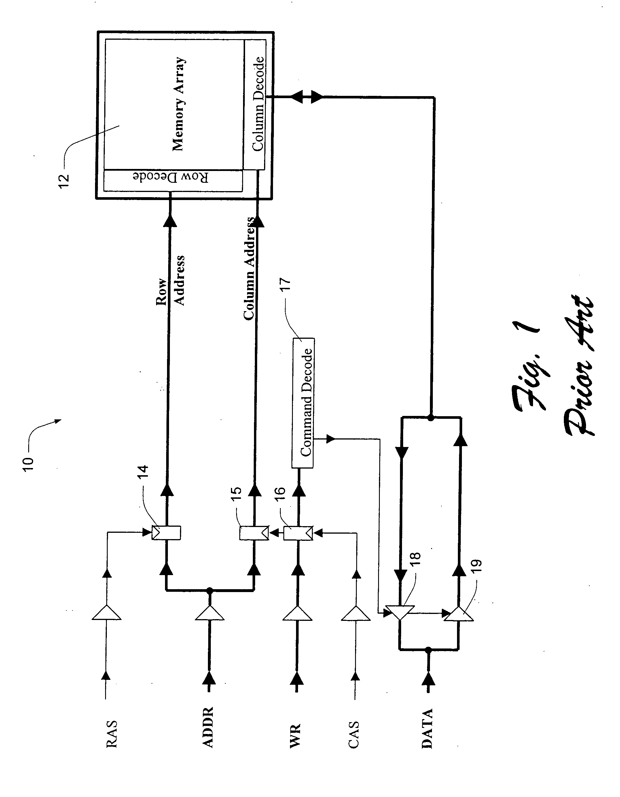
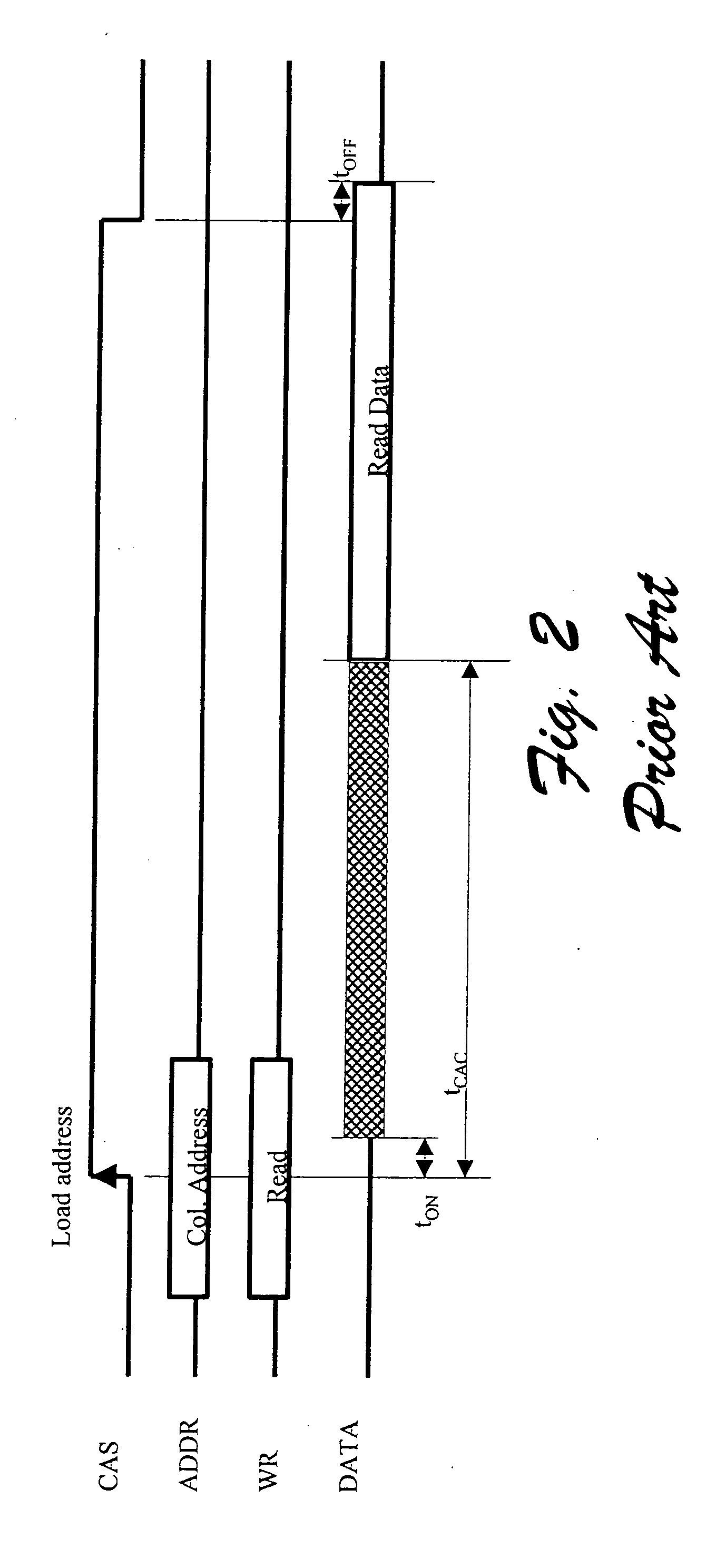
a timing element and asynchronous technology, applied in the direction of information storage, static storage, digital storage, etc., can solve the problems of high latency, quantizing internal delays, and relatively limited number of read operations per unit of tim
- Summary
- Abstract
- Description
- Claims
- Application Information
AI Technical Summary
Benefits of technology
Problems solved by technology
Method used
Image
Examples
first embodiment
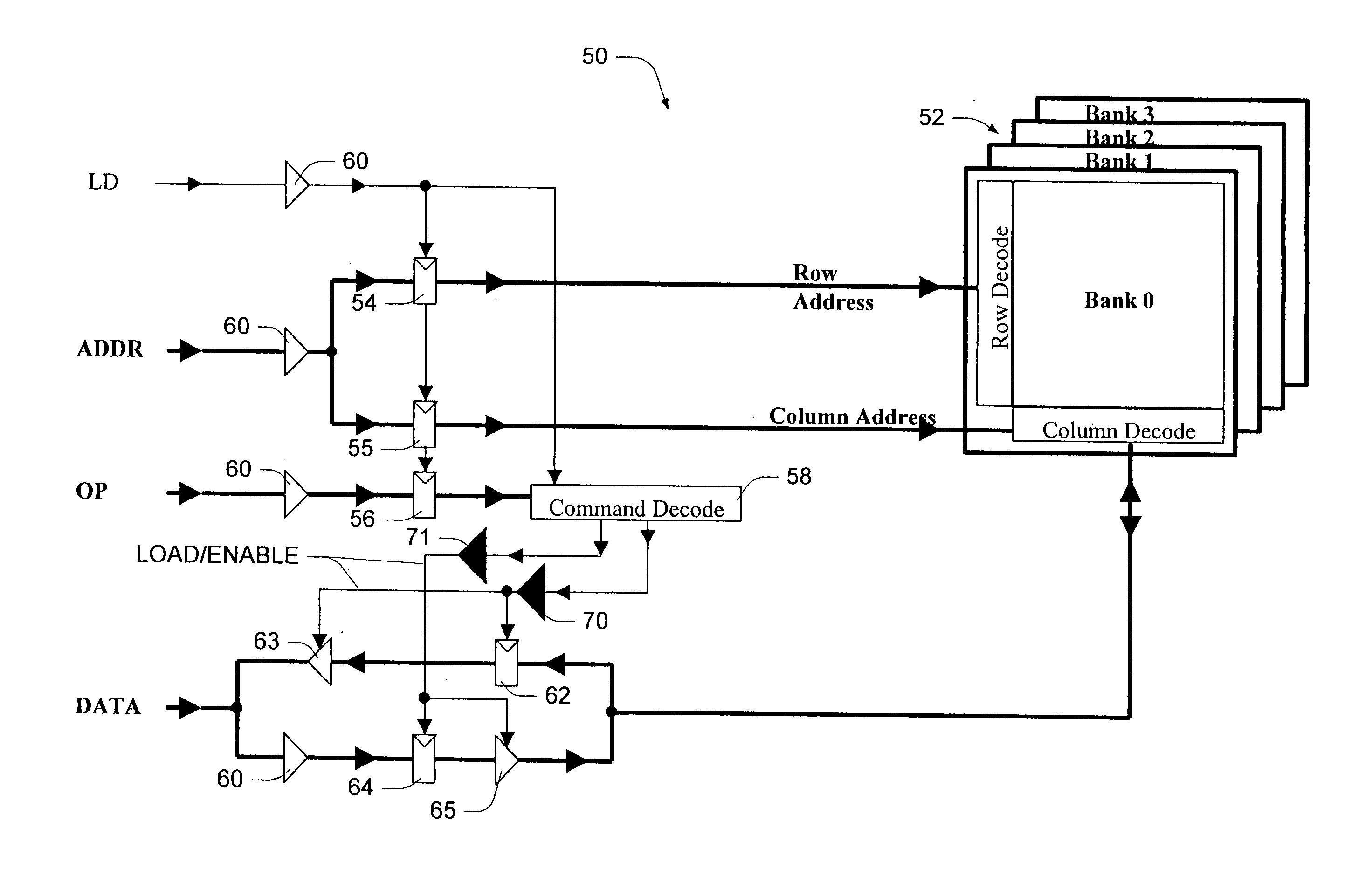
[0058]FIG. 6 shows pertinent components of an asynchronous high-speed memory device 50 which might be used in a system such as that shown in FIG. 5, or in other types of memory systems. The architecture shown in FIG. 6 allows asynchronous data transfer while still allowing data pipelining.
[0059] This example is a DRAM, but the concepts described herein are applicable to various different kinds of volatile, non-volatile, random access, and read-only memory, including SRAM (static random access memory); flash memory; mask-programmable, memory; field-programmable memory; electrically-erasable, programmable, memory; ferro-electric memory; magneto-resistive memory, etc.
[0060] Furthermore, while certain aspects of the described circuits utilize asynchronously generated signals, it is contemplated that the described asynchronous techniques might be employed in circuits that also utilize or receive periodic clock signals for certain purposes.
[0061] DRAM 50 comprises a plurality of memory...
second embodiment
with Additional Pipeline Element
[0078]FIG. 8 shows a different embodiment of a memory device, referenced by numeral 80. For the most part, this embodiment is identical to that of FIG. 5, and identical reference numerals have therefore been used to indicate identical elements. The difference in this embodiment is an additional stage of pipelining, relating to column addressing. Specifically, an additional address pipeline register 81 has been added between column address register 55 and memory core 52. This register is loaded by its own LOAD signal, which is derived or created by delaying the input load signal LD. Specifically, a delay element 82 receives the LD signal during operations involving column addresses, and delays the LD signal by an appropriate, predetermined amount.
[0079]FIG. 9 shows timing for a read cycle in the embodiment of FIG. 8. The input load signal LD initiates the memory access cycle. Again, this signal is not a periodic clock but a single transition. Subseque...
third embodiment
with Received Data Register Load
[0099]FIG. 14 shows yet another embodiment of an asynchronous memory device, referenced by numeral 110. For the most part, this embodiment is identical to that of FIG. 6, and identical reference numerals have therefore been used to indicate identical elements. The difference in the embodiment of FIG. 14 is that the delay elements have been omitted. Instead, DRAM 80 accepts two externally-supplied input load signals: LD1 and LD2. First input load signal LD1 is the same as the single LD signal of FIG. 5: it loads addresses into address registers 54 and 55, and loads a command into register 56.
[0100] Second input load signal LD2, also referred to herein as a data register load signal, is used in place of the delay element outputs. The memory controller, which generates LD2, has its own timing elements that delay LD2 relative to LD1. During a read cycle, LD2 is gated to form a LOAD / ENABLE signal that loads read data register 62. Output driver 63 is respo...
PUM
 Abstract
Description
Claims
Application Information
 - R&D
- Intellectual Property
- Life Sciences
- Materials
- Tech Scout
- Unparalleled Data Quality
- Higher Quality Content
- 60% Fewer Hallucinations
Browse by: Latest US Patents, China's latest patents, Technical Efficacy Thesaurus, Application Domain, Technology Topic, Popular Technical Reports.
© 2025 PatSnap. All rights reserved.Legal|Privacy policy|Modern Slavery Act Transparency Statement|Sitemap|About US| Contact US: help@patsnap.com


