
Board mounting method and mounting structure

Inactive Publication Date: 2005-10-20
FUJITSU LTD
View PDF17 Cites 1 Cited by
  • Summary
  • Abstract
  • Description
  • Claims
  • Application Information

AI Technical Summary

Benefits of technology

[0021] The present invention has been made in the light of such problems, and it is therefore an object of the present invention to provide a board mounting method and a mounting structure in which a distance between electronic components or between an electronic component and a board can be reduced to prevent delay in response, and also in which a large cooling component can be mounted on an electronic component in order to cool the electronic component.
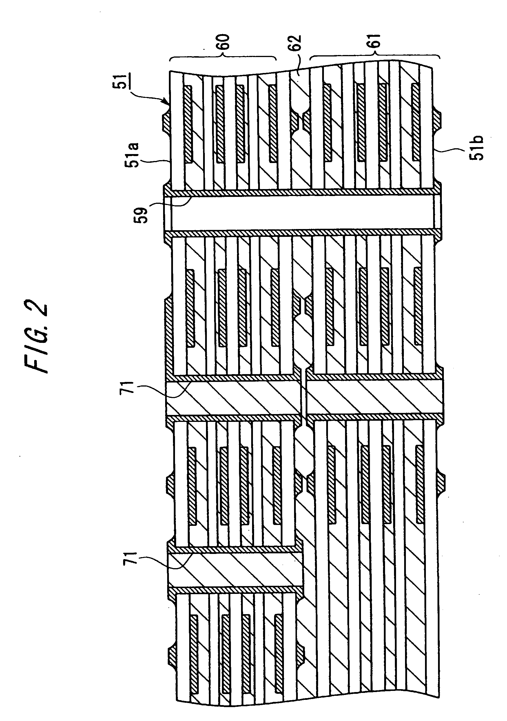
[0024] According to the present invention, the first electronic component and the second electronic component are respectively mounted on both faces of the bonded board which is formed of at least two sheets of boards bonded to and insulated from each other, and the first and second electronic components are connected through the through hole. Hence, a distance between the electronic components can be reduced as compared with the case where the first and second electronic components are mounted on a single face of the board.
[0026] In this case, even when a height of the second electronic component mounted on the bonded board is high, it is possible to prevent the second electronic component from interfering with the different board.
[0029] In this case, even when a large cooling component is mounted on the first electronic component, it is possible to prevent the large cooling component from interfering with the different board.
[0036] Further, it is possible to modularize the bonded board, the first electronic component, and the second electronic component.
[0038] In this case, the power source supply response to a load change in voltage supplied to the first electronic component is improved.

Problems solved by technology

Accordingly, heretofore, there has been a problem in that a response of each of the DD converters 13 to a load change in voltage is delayed.
When the response of each of the DD converters 113 is delayed, it is necessary to mount an electrolytic capacitor or the like, which leads to a problem of cost increase.
In addition, since the DD converters 13 are mounted outside the heat sink 14, the distance between the CPU 12 and each of the DD converters 13 increases, which leads to a problem in that the response is delayed.
In this case, the DD converters 13 need to be mounted in a position as close to the CPU 12 as possible, which leads to a problem in that it is impossible to secure a space for a large heat sink 14 to be mounted on the CPU 12.
For this reason, there has been a problem in that it is difficult to mount the large heat sink 14 having a sufficient cooling ability when the CPU 12 having a high exothermic quantity is used.
In this case, there has been a problem in that a signal transmission distance between the module board 11 and the motherboard 15 increases, and thus the response is delayed.
Hence, there has been a problem in that the distance between the CPU 12 and each of the DD converters 13 increases, and thus the response is delayed.
Also, there has been another problem in that the large heat sink 14 can not be mounted on the CPU 12.

Method used


Image

  • Board mounting method and mounting structure
  • Board mounting method and mounting structure
  • Board mounting method and mounting structure

Examples


first embodiment

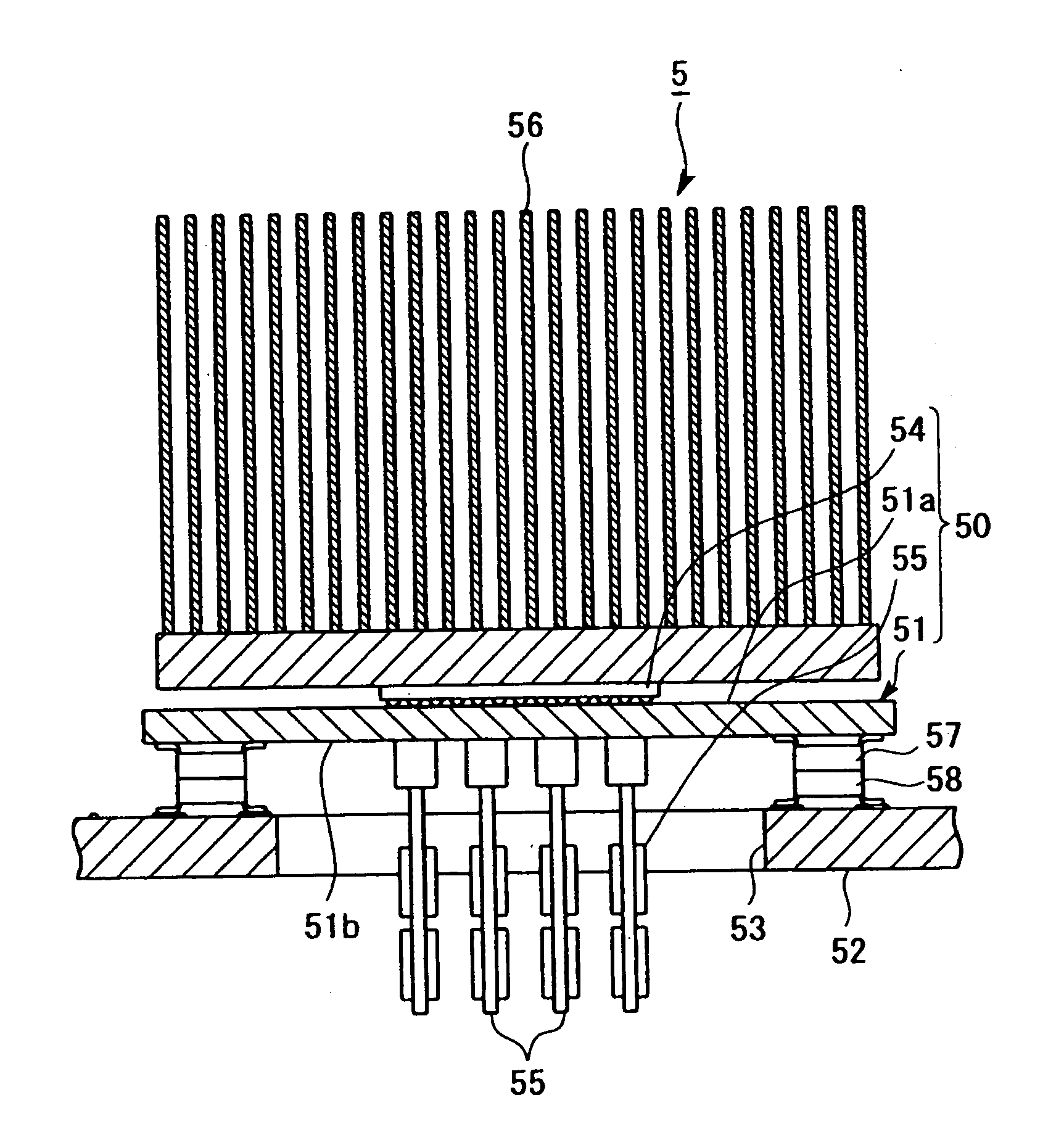
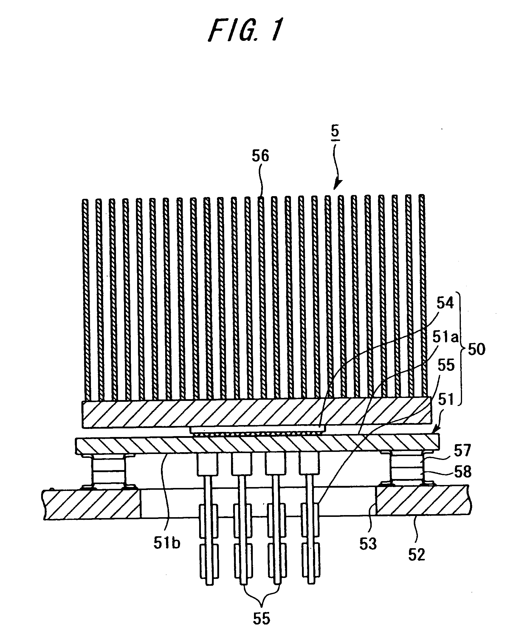
[0059]FIG. 1 shows a board mounting structure Sofa first embodiment according to the present invention. The board mounting structure 5 includes a module board 51 as a bonded board, a motherboard 52 as a different board on which the module board 51 is mounted, and an opening 53 which is formed in the motherboard 52.

[0060] In addition, the board mounting structure 5 includes a large-scale integrated circuit (LSI), i.e., a CPU 54 in this example as a first electronic component which is mounted on one face 51a of the module board 51; a DD (DC-DC) converter 55 as a second electronic component which is mounted on the other face 51b of the module board 51 and is inserted into the opening 53 of the motherboard 52; and a heat sink 56 as a cooling component which is directly mounted on the CPU 54.

[0061] The module board 51, the CPU 54, and the DD converters 55 are packaged in the form of a CPU module 50. In addition, the CPU 54, the DD converters 55, and the heat sink 56 are joined through ...

second embodiment

[0084]FIG. 7 shows a board mounting structure 6 of a second embodiment according to the present invention. Note that the same constituent elements as those of the board mounting structure 5 shown in FIG. 1 are designated with the same symbols, and their detailed descriptions are omitted here.

[0085] In the board mounting structure 6, the above-mentioned CPU module 50 is inverted in its direction to be mounted on the motherboard 52.

[0086] That is, the face 51a of the module board 51 on which the CPU 54 is mounted is disposed to be opposed to the motherboard 52. Then, the heat sink 56 mounted on the CPU 54 is inserted into the opening 53 of the motherboard 52.

[0087] In the case of the board mounting structure 6, similarly to the foregoing, the space defined by the module board 51 and the motherboard 52 can be made small. Accordingly, it is possible to prevent the signal transmission distance between the module board 51 and the motherboard 52 from being increased. Moreover, the overa...

third embodiment

[0088]FIG. 8 shows a board mounting structure 7 of a third embodiment according to the present invention. Note that the same constituent elements as those of the board mounting structure 5 shown in FIG. 1 are designated with the same symbols and their detailed descriptions are omitted here.

[0089] In the board mounting structure 7, a liquid cooling device 67 is mounted, instead of the heat sink 56 of the board mounting structure 5 shown in FIG. 1, on the CPU 54. Pipes 68 through which liquid is supplied and discharged are respectively connected to both sides of the liquid cooling device 67 through joints 69.

[0090] The board mounting structure 7 allows a wide space to be secured in the periphery of the CPU 54. Accordingly, the large liquid cooling device 67 can be mounted.

[0091] In addition, though the pipes 68 respectively extend laterally from both sides of the large liquid cooling device 67, it is possible to prevent the pipes 68 from interfering with the DD converters 55.


PUM


Abstract

A bonded board is formed by bonding at least two boards via an insulation member. A through hole is formed in the bonded board to mount a firs electronic component on one face of the bonded board, and a second electronic component on the other face of the bonded board. The first electronic component and the second electronic component are electrically connected via the through hole.

Description

BACKGROUND OF THE INVENTION [0001] 1. Technical Field [0002] The present invention relates to a board mounting method and a mounting structure which are suitable for an electronic computer, a communication apparatus, or the like. [0003] 2. Background Art [0004] There is a central processing unit (CPU) module in which a CPU and DC-DC (DD) converters are mounted on a module board. FIG. 13 shows a conventional CPU module 10. In the CPU module 10, a CPU 12 (refer to FIG. 15), and DD converters 13 are mounted on one side of a module board 11. A heat sink 14 is directly mounted on the CPU 12. [0005] The CPU module 10, as shown in FIG. 14, is mounted on a motherboard 15. RAMs 16 and I / O connectors 17 are also mounted on the motherboard 15. [0006] The module board 11 of the CPU module 10, as shown in FIG. 15, is disposed substantially in parallel with the motherboard 15. Then, the module board 11 is connected to the motherboard 15 through a module side connector 18 and a motherboard side co...

Claims


Application Information

Patent Timeline
IPC IPC(8): H05K1/14H05K1/18H05K3/36
CPCH05K1/141H05K1/182H05K2203/1572H05K2201/045H05K2201/09072H05K3/366H01L2224/16225H01L2224/73253
Inventor MORITA, YOSHIHIROUZUKA, YOSHINORI
Owner FUJITSU LTD
Learn More