Plasma display panel driver and plasma display
a plasma display panel and driver technology, applied in the direction of instruments, static indicating devices, etc., can solve the problems of difficult to establish the compatibility between the reduction of power consumption and the improvement of miniaturization, the difficulty of reducing the resistance of the separation switching device, and the further difficulty of lowering the conduction loss at so as to reduce the number of separation switching devices, reduce the withstand voltage of the separation switching device, and improve the effect of miniaturization
- Summary
- Abstract
- Description
- Claims
- Application Information
AI Technical Summary
Benefits of technology
Problems solved by technology
Method used
Image


Examples
embodiment 1
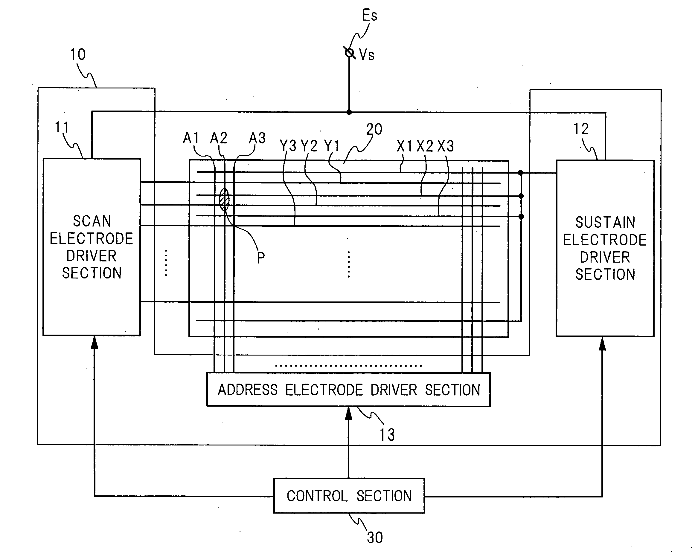
[0099] A plasma display according to Embodiment 1 of the invention comprises a PDP driver 10, a PDP 20, and a control section 30. See FIG. 1.
[0100] The PDP 20 is an AC type, for example, and comprises the three-electrode surface-discharge type structure. Address electrodes A1, A2, A3, . . . are arranged on the rear substrate of the PDP 20 in the vertical direction of the panel. Sustain electrodes X1, X2, X3, . . . and scan electrodes Y1, Y2, Y3, . . . are alternately arranged on the front substrate of the PDP 20 in the horizontal direction of the panel. The sustain electrodes X1, X2, X3, . . . are connected to each other, and thus, have a substantially equal potential. The address electrodes A1, A2, A3, . . . and the scan electrodes Y1, Y2, Y3, . . . each allow an individual potential change.
[0101] A discharge cell is installed at the intersection of an adjacent pair of sustain and scan electrodes (e.g., a pair of sustain and scan electrodes X2 and Y2) and an address electrode (e....
embodiment 2
[0154] A plasma display according to Embodiment 2 of the invention comprises a configuration quite similar to that of the above-described plasma display according to Embodiment 1 (cf. FIG. 1). Accordingly, for the details of the configuration, the explanation of the above-described Embodiment 1 and FIG. 1 are cited.
[0155] A sustain electrode driver section according to Embodiment 2 of the invention (not shown) comprises a configuration quite similar to that of the sustain electrode driver section 12 according to Embodiment 1 (cf. FIG. 2). Accordingly, for the details of the configuration, the explanation of Embodiment 1 and FIG. 2 are cited.
[0156] In a scan electrode driver section 11 according to Embodiment 2 of the invention, a reset pulse generating section 2B includes an negative voltage source En and a second bypass switching device QB2, in contrast to the reset pulse generating section 2A according to Embodiment 1 (cf. FIG. 2). See FIGS. 5 and 6. Furthermore, a first separat...
embodiment 3
[0178] A plasma display according to Embodiment 3 of the invention comprises a configuration quite similar to that of the above-described plasma display according to Embodiment 1 (cf. FIG. 1). Accordingly, for the details of the configuration, the explanation of the above-described Embodiment 1 and FIG. 1 are cited.
[0179] A sustain electrode driver section according to Embodiment 3 of the invention (not shown) comprises a configuration quite similar to that of the sustain electrode driver section 12 according to Embodiment 1 (cf. FIG. 2). Accordingly, for the details of the configuration, the explanation of Embodiment 1 and FIG. 2 are cited.
[0180] In a scan electrode driver section 11 according to Embodiment 3 of the invention, a scan pulse generating section 1B includes no first bypass switching device QB1, in contrast to the scan pulse generating sections 1A according to Embodiments 1 and 2 (cf. FIGS. 2, 5, and 6). See FIGS. 8-11. In other words, the positive electrode of the fi...
PUM
 Abstract
Description
Claims
Application Information
 - R&D
- Intellectual Property
- Life Sciences
- Materials
- Tech Scout
- Unparalleled Data Quality
- Higher Quality Content
- 60% Fewer Hallucinations
Browse by: Latest US Patents, China's latest patents, Technical Efficacy Thesaurus, Application Domain, Technology Topic, Popular Technical Reports.
© 2025 PatSnap. All rights reserved.Legal|Privacy policy|Modern Slavery Act Transparency Statement|Sitemap|About US| Contact US: help@patsnap.com