Flash memory cell transistor and method for fabricating the same

a technology of flash memory cell and transistor, which is applied in the direction of transistors, electrical devices, semiconductor devices, etc., can solve the problems of gate oxide film thickness becoming thinner, and it is difficult to fabricate a pmos transistor in the prior ar

Inactive Publication Date: 2005-10-20
SK HYNIX INC
View PDF0 Cites 5 Cited by
  • Summary
  • Abstract
  • Description
  • Claims
  • Application Information

AI Technical Summary

Benefits of technology

[0021] Accordingly, it is an object of the present invention to provide a flash memory cell transistor comprising a nMOS region and a pMOS region which are formed of the same n+ polysilicon, where a gate oxide film is used in the nMOS region and a triple gate insu

Problems solved by technology

As a result, it is difficult to fabricate a pMOS transistor in the prior art since the PMOS transistor having the channel length of less than 0.15 μm has a large short channel effect.
When the p+ polys

Method used


Image

  • Flash memory cell transistor and method for fabricating the same
  • Flash memory cell transistor and method for fabricating the same
  • Flash memory cell transistor and method for fabricating the same

Examples


Embodiment Construction

[0037] The present invention will be described in detail with reference to the accompanying drawings.

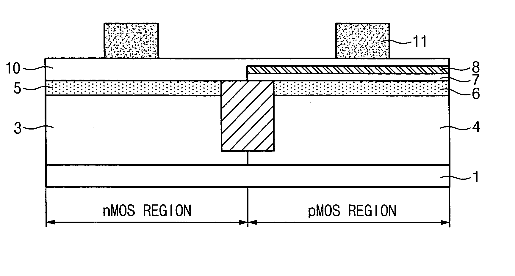
[0038] In an embodiment, as shown in FIG. 5, a p-well region 3 and a n-well region 4 which are divided by an isolation oxide film region 2 are formed on a silicon substrate 1. A nMOS channel ion-implantation region 5 is formed on the p-well region 3, and a second gate oxide film 9 is formed on the nMOS channel ion-implantation region 5, and a n+ polysilicon gate electrode is formed on the second gate oxide film 9. Additionally, a pMOS channel ion-implantation region 6 is formed on the n-well region 4. Then, a first gate oxide film 7, an insulating film 8 having an electron trap and a second gate oxide film 9 are sequentially formed on the pMOs channel ion-implantation region 6. The n+ polysilicon gate electrode 10 is formed thereon.

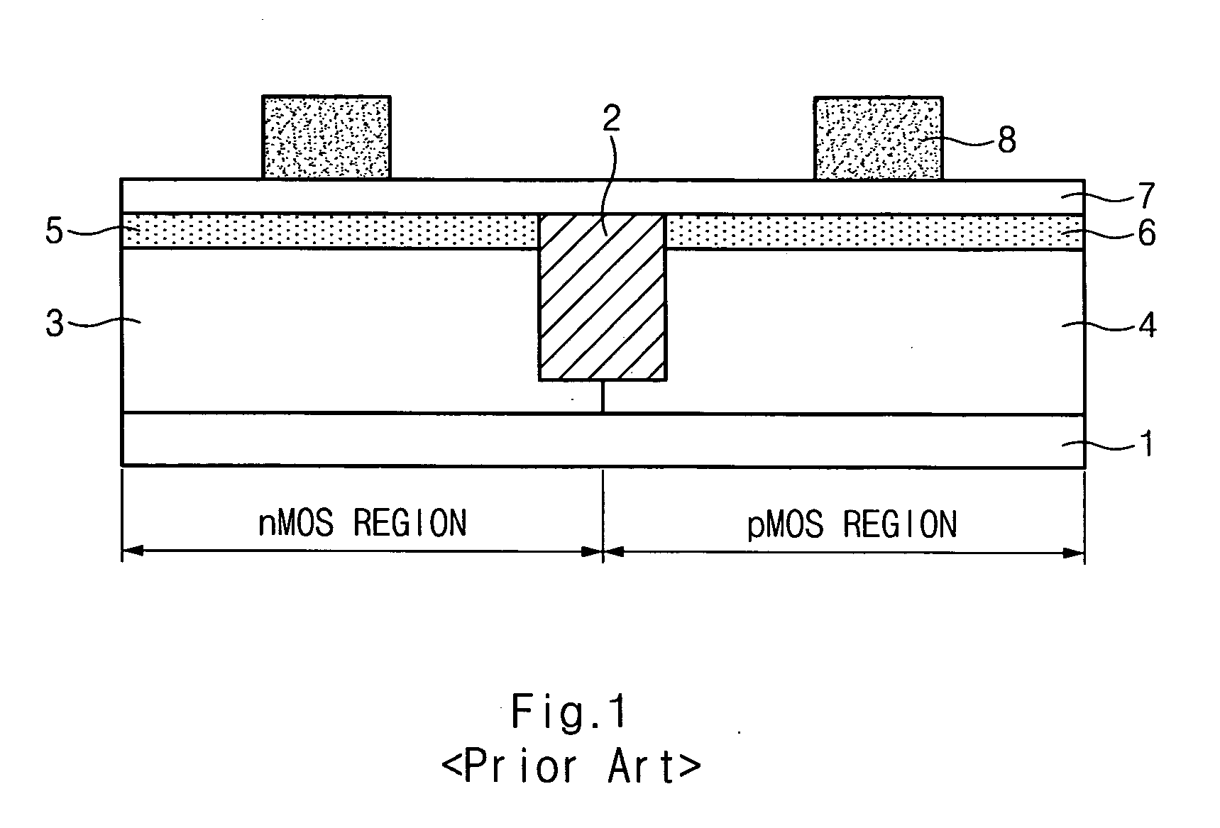
[0039] In the above-described transistor of FIG. 5, although the same n+ polysilicon is used to the nMOS region and the pMOS region (see FIG. 1), only t...


PUM


Abstract

A flash memory cell transistor and a method for fabricating the same compensates a work function difference of a MOS and a nMOS with a triple gate insualting film by using electron density trapped in a pMOS gate insulating film. The flash memory cell transistor comprises a p-well region and a n-well region. The nMOS region comprises a nMOS channel ion-implantation region on the p-well region, a second gate oxide film on the nMOS channel ion-implantation region and a first n+ polysilicon gate electrode on the second gate oxide film. The pMOS region comprises a MOS channel ion-implantation region on the n-well region, a first gate oxide film, an insulating film having an electron trap and the second gate oxide film which are sequentially formed on the PMOS channel ion-implantation region, and a second n+ polysilicon gate electrode on the second gate oxide film.

Description

BACKGROUND OF THE INVENTION [0001] 1. Field of the Invention [0002] The present invention generally relates to a flash memory cell transistor, and more specifically, to a flash memory cell transistor which compensates a difference in work function of pMOS and nMOS with a triple gate insulating film by using electron density trapped in a pMOS gate insulating film. [0003] 2. Description of the Prior Art [0004]FIG. 1 is a cross-sectional diagram illustrating an example of a conventional flash memory cell transistor. [0005] Referring to FIG. 1, a n-well 4 and a p-well 3 are formed on a silicon substrate 1, and an isolation oxide film 2 is formed between the n-well 4 and the p-well 3. The flash memory cell transistor of FIG. 1 that has a structure of a CMOS transistor comprises a nMOS region and a pMOS region. In the nMOS region, a nMOS ion-implantation region 5, a gate oxide film 7 and a n+ polysilicon gate electrode 8 are sequentially formed on the p-well 3. In the PMOS region, a pMOS ...

Claims


Application Information

Patent Timeline
IPC IPC(8): H01L21/8238H01L21/8246H01L27/115H01L29/788
CPCH01L21/823857H01L27/11568H01L27/115H10B43/30H10B69/00H01L21/823828
Inventor LEE, SANG DON
Owner SK HYNIX INC
Why Eureka
Try Eureka