Nanowire light emitting device and method of fabricating the same

Inactive Publication Date: 2005-10-13
SAMSUNG ELECTRONICS CO LTD
View PDF11 Cites 63 Cited by
  • Summary
  • Abstract
  • Description
  • Claims
  • Application Information

AI Technical Summary

Benefits of technology

[0016] The p-doping or n-doping of the lower portion of the nanowires may comprise: adsorbing molecules having a high electric affinity or a low ionization potential around a circumference of the nanowires; filling a first insulating polymer between the nanowires on the first electrode layer; and removing the molecules adsorbed on the upper portion of the nanowires by etching the first insulating polymer corresponding to the upper portion of the nanowires.
[0017] The n-doping or p-doping of the upper portion of the nanowires with a different polarity from that of the lower portion of the nanowires may comprise adsorbing molecules having a high electric affinity or a low ionization potential so that the different polarity portion is doped around the circumference of the nanowires exposed on the lower portion of th

Problems solved by technology

Although the GaN-based LED has high light emitting efficiency, it has a mismatch problem with a substrate, thus making it difficult to be used for producing a large size device.
The silicon nanowire light emitting device, however, has a low light emitting efficiency while being manufactured at a low cost.
As the nanowire light emitting device having the p-n junction structure is grown on a catalytic layer, the n-type nanowire and the p-type nanowire are sequentially formed, thus making it difficult to obtain a high quality p-n junction structure.

Method used


Image

  • Nanowire light emitting device and method of fabricating the same
  • Nanowire light emitting device and method of fabricating the same
  • Nanowire light emitting device and method of fabricating the same

Examples


Embodiment Construction

[0023] A nanowire light emitting device and a method of fabricating the same according to the present invention will become more apparent by describing in detail exemplary embodiments thereof with reference to the attached drawings.

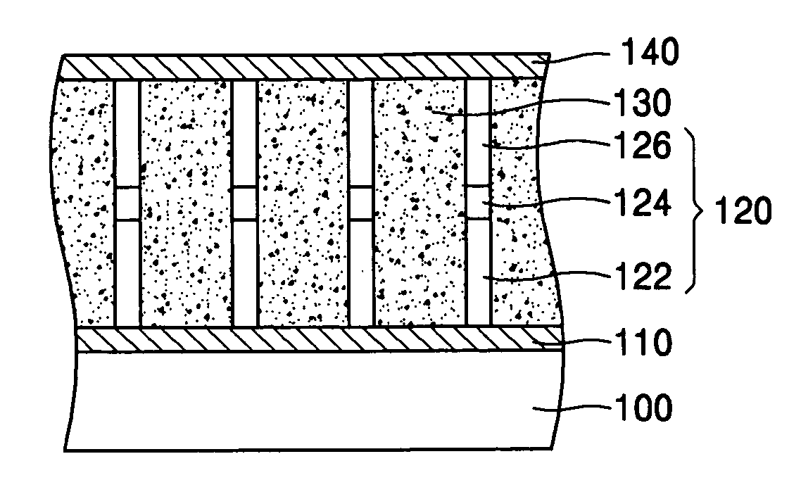
[0024]FIG. 1 is a cross-sectional view of a nanowire light emitting device according to a first exemplary embodiment of the present invention.

[0025] Referring to FIG. 1, a conductive layer (a first electrode layer) 110 is formed on a substrate 100 and a plurality of nanowires 120 are vertically formed on the conductive layer 110. An insulating polymer 130 is filled in a space between the nanowires 120. An electrode layer (a second electrode layer) 140 is formed on the nanowires 120.

[0026] The nanowires 120 are composed of a p-type doped portion 122, an n-type doped portion 126, and an intrinsic portion 124, being a light emitting layer between the p-type doped portion 122 and the n-type doped portion 126. The intrinsic portion is not doped.

[0027] The ...


PUM


Abstract

A nanowire light emitting device and a method of fabricating the same are provided. The nanowire light emitting device includes a first conductive layer on a substrate, a plurality of nanowires on the first conductive layer, each nanowire having a p-type doped portion and an n-type doped portion on both ends, a light emitting layer between the p-type doped portion and n-type doped portion, and a second conductive layer formed on the nanowires. The doped portions are formed by adsorbing molecules around a circumference thereof.

Description

[0001] This application claims priority from Korean Patent Application No. 10-2004-0023803, filed on Apr. 7, 2004, in the Korean Intellectual Property Office, the disclosure of which is incorporated herein in its entirety by reference. BACKGROUND OF THE INVENTION [0002] 1. Field of the Invention [0003] The present invention relates to a nanowire light emitting device and a method of fabricating the same, and more particularly, to a nanowire light emitting device producible at a low manufacturing cost and which can be used for forming a large size device and a method of fabricating the nanowire light emitting device. [0004] 2. Description of the Related Art [0005] A light emitting diode (LED) using gallium nitride (GaN) is used as a light emitting device. Although the GaN-based LED has high light emitting efficiency, it has a mismatch problem with a substrate, thus making it difficult to be used for producing a large size device. [0006] Technologies using nanostructures for light emi...

Claims


Application Information

Patent Timeline
IPC IPC(8): H01L29/06H01L27/15H01L33/28H01L33/36
CPCB82Y20/00H01L33/08H01L33/18H01L33/24B82Y10/00H01L29/06
Inventor JIN, YOUNG-GULEE, SUNG-HOONLEE, HYO-SUGCHOI, BYOUNG-IYONGKIM, JONG-SEOB
Owner SAMSUNG ELECTRONICS CO LTD
Why Eureka
Try Eureka