Eureka AIR delivers breakthrough ideas for toughest innovation challenges, trusted by R&D personnel around the world.

Adaptive sampling method for improved control in semiconductor manufacturing

a sampling method and semiconductor technology, applied in semiconductor/solid-state device testing/measurement, electric controllers, instruments, etc., can solve problems such as engendering nonoptimal control of critical processing parameters, many of the processing tools currently commercially available suffer certain deficiencies, and many tools lack advanced process data monitoring capabilities

Inactive Publication Date: 2005-10-06
ADVANCED MICRO DEVICES INC
View PDF8 Cites 80 Cited by
  • Summary
  • Abstract
  • Description
  • Claims
  • Application Information

AI Technical Summary

Benefits of technology

[0014] In one aspect of the present invention, a method is provided, the method comprising sampling at least one parameter characteristic of processing performed on a workpiece in at least one processing step, and modeling the at least one characteristic parameter sampled using an adaptive sampling processing model, treating sampling as an integrated part of a dynamic control environment, varying the sampling based upon at least one of situational information, upstream events and requirements of run-to-run controllers. The method also comprises applying the adaptive sampling processing model to modify the processing performed in the at least one processing step.
[0015] In another aspect of the present invention, a computer-readable, program storage device is provided, encoded with instructions that, when executed by a computer, perform a method, the method comprising sampling at least one parameter characteristic of processing performed on a workpiece in at least one processing step, and modeling the at least one characteristic parameter sampled using an adaptive sampling processing model, treating sampling as an integrated part of a dynamic control environment, varying the sampling based upon at least one of situational information, upstream events and requirements of run-to-run controllers. The method also comprises applying the adaptive sampling processing model to modify the processing performed in the at least one processing step.
[0016] In yet another aspect of the present invention, a computer programmed to perform a method is provided, the method comprising sampling at least one parameter characteristic of processing performed on a workpiece in at least one processing step, and modeling the at least one characteristic parameter sampled using an adaptive samplin

Problems solved by technology

However, despite the advances made in this area, many of the processing tools that are currently commercially available suffer certain deficiencies.
In particular, such tools often lack advanced process data monitoring capabilities, such as the ability to provide historical parametric data in a user-friendly format, as well as event logging, real-time graphical display of both current processing parameters and the processing parameters of the entire run, and remote, i.e., local site and worldwide, monitoring.
These deficiencies can engender nonoptimal control of critical processing parameters, such as throughput accuracy, stability and repeatability, processing temperatures, mechanical tool parameters, and the like.
Run-to-run control as practiced in high-volume, multi-product semiconductor manufacturing does not easily fit into the framework of traditional approaches to process control.
One reason this approach is not always applicable is that there are often multiple processing tools as well as multiple products.
Determining how to do controller updates in this environment can be a challenging task.
When the various processes run on the tool are significantly different, the controller may behave unexpectedly because a change to a new process can appear to be a large disturbance.
In addition, it may take several successive runs of a given process for the controller to stabilize, but manufacturing constraints may prevent this from happening.
Thus, one of the many control problems is to determine the optimal settings for each product / layer / tool combination that arises.
The rapid thermal processing (RTP) performance typically degrades with consecutive process runs, in part due to drift in the respective settings of the rapid thermal processing (RTP) tool and / or the rapid thermal processing (RTP) sensors.
This may cause differences in wafer processing between successive runs or batches or lots of wafers, leading to decreased satisfactory wafer throughput, decreased reliability, decreased precision and decreased accuracy in the semiconductor manufacturing process.
However, traditional statistical process control (SPC) techniques are often inadequate to control precisely process parameters related to rapid thermal processing (RTP) in semiconductor and microelectronic device manufacturing so as to optimize device performance and yield.
Furthermore, blindly minimizing non-adaptive processing spreads about target values may not increase processing yield and throughput.
Traditional control techniques are frequently ineffective in reducing off-target processing and in improving sort yields.
When one or more of the processing steps are producing resulting wafers that the wafer electrical test (WET) measurements indicate are unacceptable, causing the resulting wafers to be scrapped, this misprocessing goes undetected and uncorrected for quite a while, often for weeks, leading to many scrapped wafers, much wasted material and decreased overall throughput.
Metrology operations require a significant amount of capital and consume large amounts of cycle time in semiconductor manufacturing.

Method used


Image

  • Adaptive sampling method for improved control in semiconductor manufacturing
  • Adaptive sampling method for improved control in semiconductor manufacturing
  • Adaptive sampling method for improved control in semiconductor manufacturing

Examples


Embodiment Construction

[0038] Illustrative embodiments of the invention are described below. In the interest of clarity, not all features of an actual implementation are described in this specification. It will of course be appreciated that in the development of any such actual embodiment, numerous implementation-specific decisions must be made to achieve the developers' specific goals, such as compliance with system-related and business-related constraints, which will vary from one implementation to another. Moreover, it will be appreciated that such a development effort might be complex and time-consuming, but would nevertheless be a routine undertaking for those of ordinary skill in the art having the benefit of this disclosure.

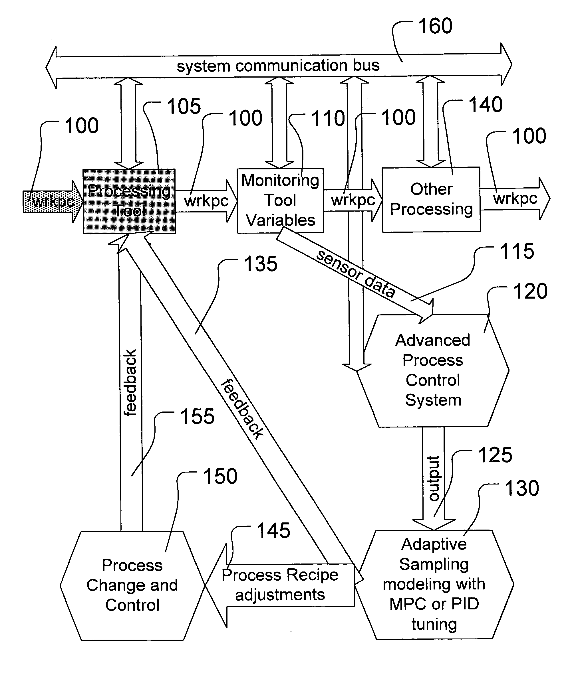
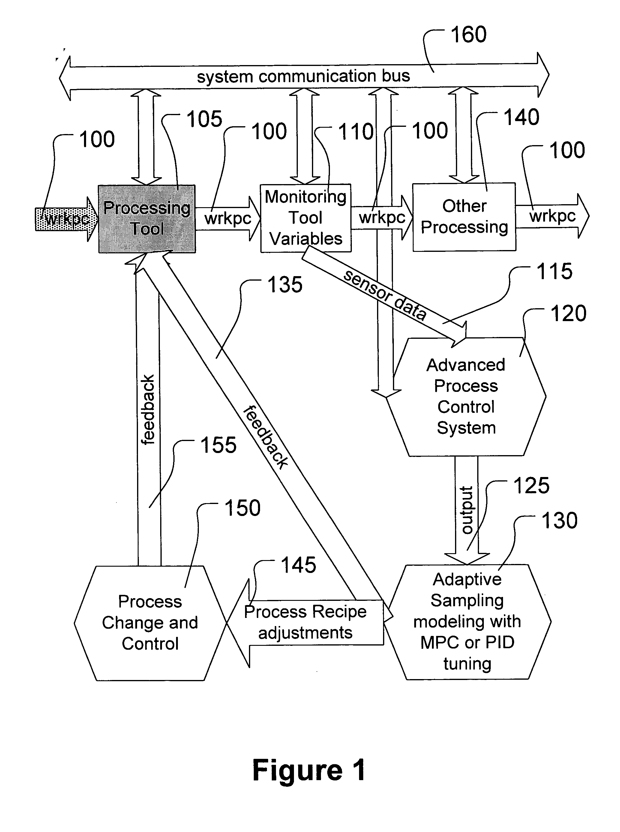
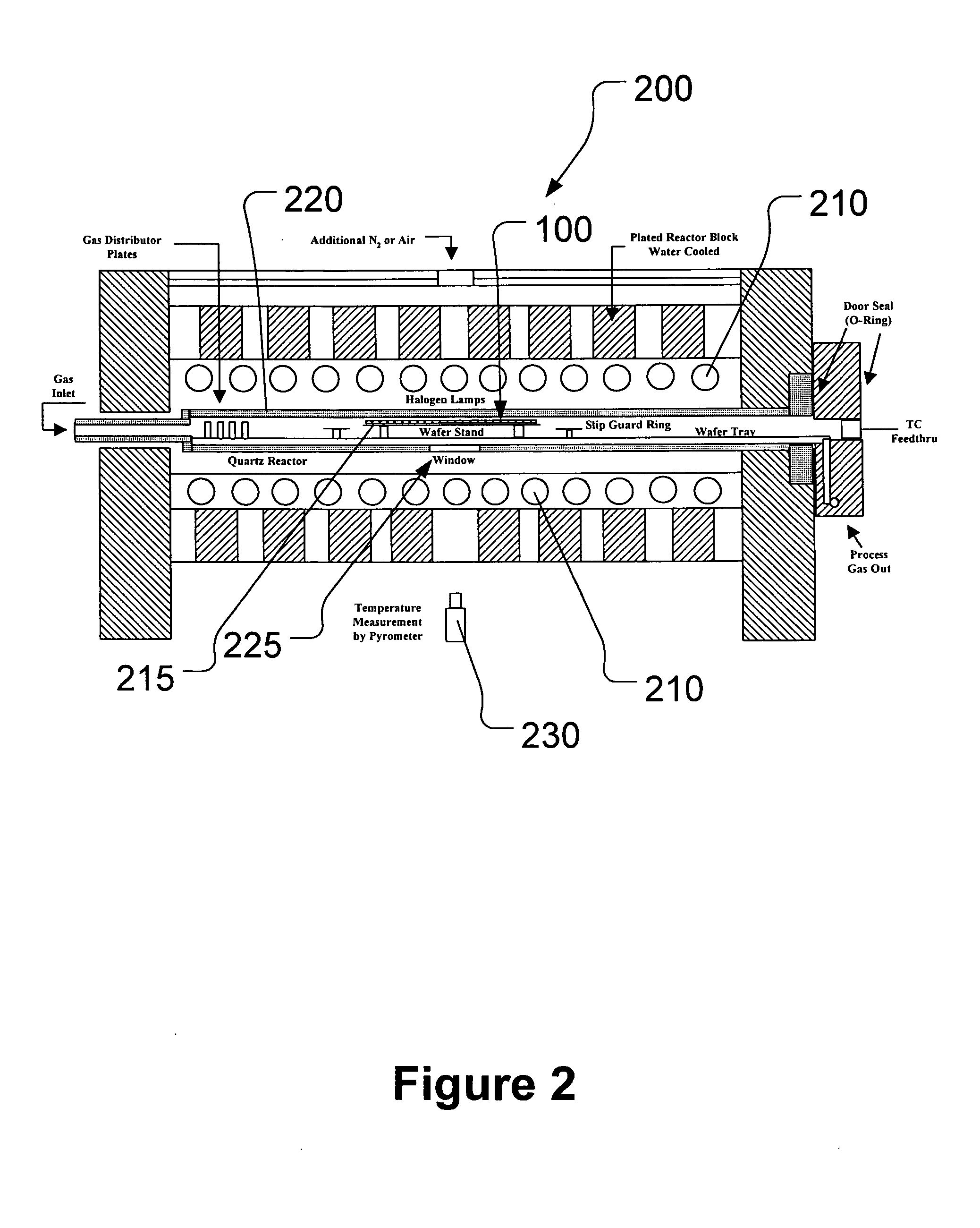
[0039] Illustrative embodiments of a method according to the present invention are shown in FIGS. 1-30. As shown in FIG. 1, a workpiece 100, such as a semiconducting substrate or wafer, having zero, one, or more process layers and / or semiconductor devices, such as a metal-oxide...


PUM


Abstract

A method is provided, the method comprising sampling at least one parameter characteristic of processing performed on a workpiece in at least one processing step, and modeling the at least one characteristic parameter sampled using an adaptive sampling processing model, treating sampling as an integrated part of a dynamic control environment, varying the sampling based upon at least one of situational information, upstream events and requirements of run-to-run controllers. The method also comprises applying the adaptive sampling processing model to modify the processing performed in the at least one processing step.

Description

BACKGROUND OF THE INVENTION [0001] 1. Field of the Invention [0002] This invention relates generally to semiconductor fabrication technology, and, more particularly, to a method for semiconductor fabrication supervision and optimization. [0003] 2. Description of the Related Art [0004] There is a constant drive within the semiconductor industry to increase the quality, reliability and throughput of integrated circuit devices, e.g., microprocessors, memory devices, and the like. This drive is fueled by consumer demands for higher quality computers and electronic devices that operate more reliably. These demands have resulted in a continual improvement in the manufacture of semiconductor devices, e.g., transistors, as well as in the manufacture of integrated circuit devices incorporating such transistors. Additionally, reducing defects in the manufacture of the components of a typical transistor also lowers the overall cost per transistor as well as the cost of integrated circuit devic...

Claims


Application Information

Patent Timeline
IPC IPC(8): G05B11/42G05B13/02G05B13/04H01L21/02G05B17/02G05B21/02
CPCG05B11/42G05B13/048G05B17/02G05B21/02G05B13/02
Inventor PASADYN, ALEXANDER JAMESTOPRAC, ANTHONY JOHNMILLER, MICHAEL LEE
Owner ADVANCED MICRO DEVICES INC
Why Eureka
Eureka Blog
Learn More