Front-illuminated-type photodiode array

a photodiode array and front-illuminated technology, applied in the direction of electrical equipment, semiconductor devices, radio control devices, etc., can solve the problems of deterioration of the pn junction, other problems, and inability to take optical crosstalk into account in conventional designs, so as to achieve the effect of reducing optical crosstalk

Active Publication Date: 2005-09-08
SUMITOMO ELECTRIC IND LTD
View PDF4 Cites 22 Cited by
  • Summary
  • Abstract
  • Description
  • Claims
  • Application Information

AI Technical Summary

Benefits of technology

[0027] According to the present invention, a leakage-lightwave-absorbing layer having a band gap comparable to or smaller than that of the absorption layer is provided between the rear electrode and the absorption layer. Consequently, an incoming lightwave passes through the leakage-lightwave-absorbing layer before and after being reflected from the rear electrode. That is, it is absorbed by the leakage-lightwave-absorbing layer twice and attenuates. As a result, optical crosstalk can be reduced.

Problems solved by technology

In practical applications, when the inside of the isolation grooves 22 is empty, the pn junction may deteriorate or other problems may be caused.
As a result, no conventional designs take the optical crosstalk into account.

Method used


Image

  • Front-illuminated-type photodiode array
  • Front-illuminated-type photodiode array
  • Front-illuminated-type photodiode array

Examples


example 1

One-dimensionally Arranged Photodiode Array (Above Type: M×1)

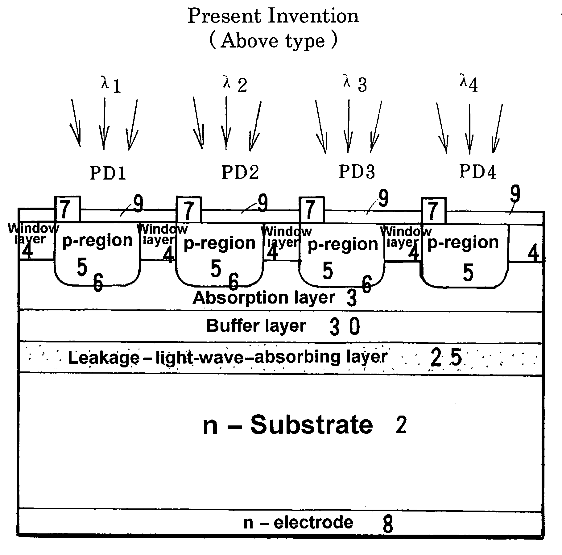
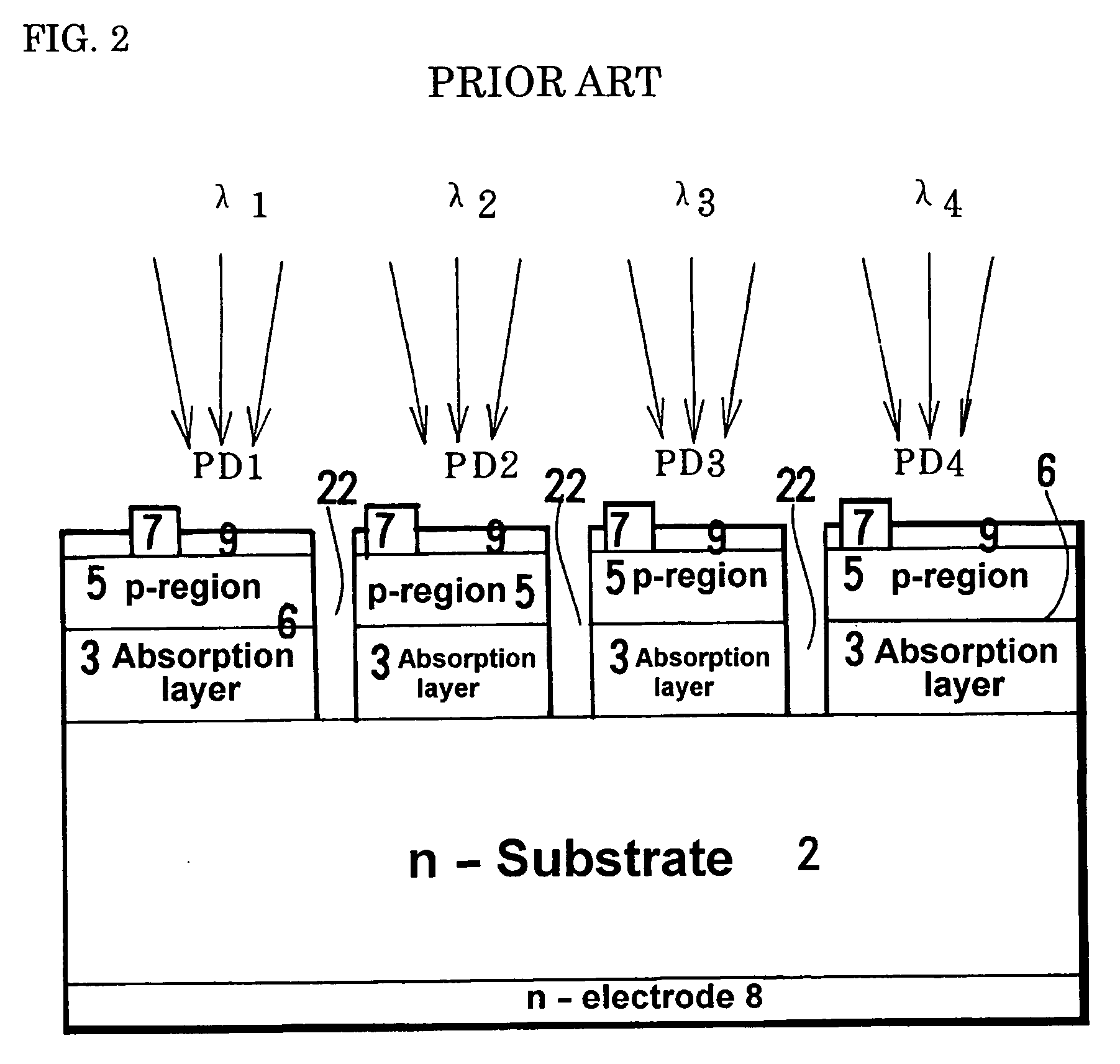
[0062] An embodiment of an above-type photodiode array of the present invention that has a leakage-lightwave-absorbing layer provided above the substrate (see FIG. 5) is explained below by referring to FIG. 9. Although FIG. 9 shows an array having four unit photodiodes, the number of unit photodiodes may be increased. When an array has a specific number of photodiode units such that the number is expressed as a power of two such as eight, 16, 32, and so on, the array is suitable for a receiving section of optical communication. It is recommended that the pitch of the arrangement be either the same as the diameter of the cladding of the optical fiber (125 μm) or an integral multiple of the diameter. For an optical sensor in which a plurality of photodiode units are arranged one-dimensionally, both the number of photodiode units M and the pitch P can be determined freely in accordance with the purpose.

[0063] In Example 1, ...

example 2

Two-dimensionally Arranged Photodiode Array (Above Type: M×N)

[0076] The present invention can also be applied to a front-illuminated-type two-dimensionally arranged photodiode array. FIG. 10 shows a partial plan view of it, and FIG. 11 a partial cross-sectional view of it. This array is formed by arranging photodiode units, “M×N” in number, on one chip. When viewed from above, p-regions 5 and p-electrodes 7 are arranged in rows and columns. Actually, the top surface is covered with an antireflective coating 9 and the p-electrodes 7 complementarily. A number of electrode pads 40 connected to the p-electrodes are provided at one, two, three, or four sides of the chip. The electrode pads 40 are connected through wires 42 to the p-electrodes 7 of the individual photodiode units. An n-electrode 8 is common and placed at the rear side of the chip. Consequently, it is bonded to a stem of a package. The electrode pads 40 are connected to pins of the package by wire bonding.

[0077] As shown...


PUM


Abstract

A front-illuminated-type photodiode array comprises (a) a first-electroconductive-type semiconductor substrate, (b) a first-electroconductive-type electrode placed at the rear-face side of the semi-conductor substrate, (c) a first-electroconductive-type absorption layer formed at the front-face side of the semiconductor substrate, (d) a plurality of second-electroconductive-type regions formed from the surface of the absorption layer to a certain distance into the absorption layer such that the regions are arranged one- or two-dimensionally, (e) a second-electroconductive-type electrode provided at part of each of the second-electroconductive-type regions, (f) an antireflective coating that covers the top surface other than the individual second-electroconductive-type electrodes and that is for preventing reflection of an incoming lightwave, and (g) at least one leakage-lightwave-absorbing layer that is provided between the first-electroconductive-type electrode and the absorption layer and that has an absorption edge wavelength, λga, equal to or longer than the absorption edge wavelength, λgr, of the absorption layer (λga≧λgr).

Description

BACKGROUND OF THE INVENTION [0001] 1. Field of the Invention [0002] The present invention relates both to a front-illuminated-type photodiode array in which a plurality of photodiode units for optical communication are unified and to a front-illuminated-type photodiode array for a sensor in which a plurality of photodiode units are arranged two- or one-dimensionally. [0003] 2. Description of the Background Art [0004] The field of optical communication has been achieving widespread adoption of the wavelength division multiplexing (WDM) technology, which enables the transmission and reception of a plurality of optical signals having different wavelengths through a single optical fiber. After the separation of the wavelength-multiplexed optical signals, in order to receive individual optical signals having a different wavelength, a plurality of independent photodiodes (PDs) arranged in parallel are sometimes used. For the same purpose, a photodiode array in which a plurality of photodi...

Claims


Application Information

Patent Timeline
Patent Type & Authority Applications(United States)
IPC IPC(8): H01L27/146H01L29/732H01L31/10
CPCH01L27/1446H01L27/14694H01L27/14629H01L27/14601
Inventor IGUCHI, YASUHIRO
Owner SUMITOMO ELECTRIC IND LTD
Why Eureka
Try Eureka