Method for patterning self-assembled colloidal photonic crystals and method for fabricating 3-dimensional photonic crystal waveguides of an inverted-opal structure using the patterning method

a technology of colloidal photonic crystals and patterning methods, which is applied in the direction of magnetic recording, chemically reactive gases, record information storage, etc., can solve the problems of difficult to form a three-dimensional photonic band gap, difficult to selectively control colloidal particles, and possible two-dimensional photonic band gaps

Active Publication Date: 2005-08-25
SAMSUNG DISPLAY CO LTD
View PDF14 Cites 11 Cited by
  • Summary
  • Abstract
  • Description
  • Claims
  • Application Information

AI Technical Summary

Problems solved by technology

However, in the wavelength ranges of infrared rays and visible light, it was only possible to form a two-dimensional photonic band gap.
This is because it was very difficult to form a three-dimensional photonic band gap due to the need for scaling-down the etching space.
However, it is difficult to selectively control the colloidal particles, and many semiconductor processes such as the lithography are required for patterning the photonic crystals.
Also, in the case of forming colloidal photonic crystals using three or more kinds of colloidal particles or colloidal particles having three or more sizes, the fabricating processes become complicated with limitations in design.
The fabrication of a waveguide having the three-dimensional photonic band gap requires a high-grade etching technique such as e-beam lithography, a high fabricating cost and considerable manufacturing time, and it is difficult to implement the waveguide in a wide area.
14, 2003, pp 271-294 by W. Lee et al. has problems due to material and area limitations.
14, 2003, pp 323-326 by P. Ferrand et al. also has problems in that its process is complicated and the photonic crystals are broken with the occurrence of cracks during an artificial piling up of the photonic crystals.

Method used


Image

  • Method for patterning self-assembled colloidal photonic crystals and method for fabricating 3-dimensional photonic crystal waveguides of an inverted-opal structure using the patterning method
  • Method for patterning self-assembled colloidal photonic crystals and method for fabricating 3-dimensional photonic crystal waveguides of an inverted-opal structure using the patterning method
  • Method for patterning self-assembled colloidal photonic crystals and method for fabricating 3-dimensional photonic crystal waveguides of an inverted-opal structure using the patterning method

Examples


first embodiment

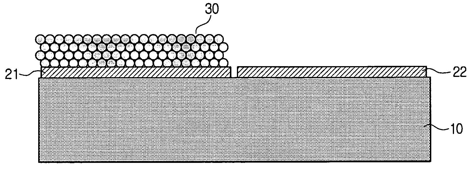
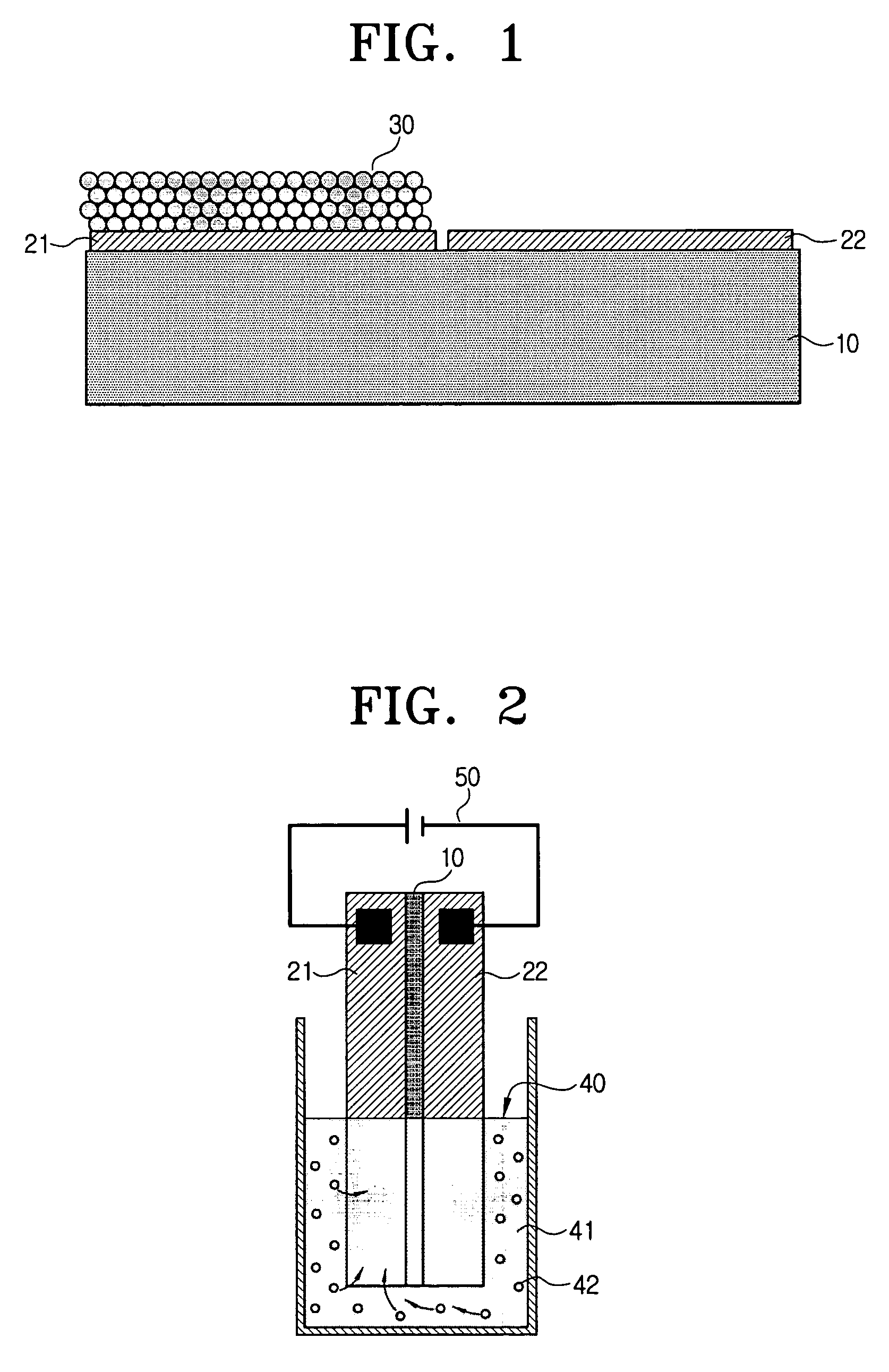
[0032]FIG. 1 is a sectional view of a self-assembled colloidal photonic crystal selectively formed on a specified area patterned on a substrate according to the present invention.

[0033] Referring to FIG. 1, a first conductive film 21 separate from a second conductive film 22 of a specified pattern are formed on a substrate 10, and a self-assembled colloidal photonic crystal 30 is formed only on the first conductive film 21.

[0034] According to the method for patterning the self-assembled colloidal structure, a position, in which the self-assembled colloidal photonic crystal is formed, is selectively determined by controlling the attractive force or repulsive force exerted between colloidal particles having a polarity and electrodes, i.e., the conductive films, by applying a voltage to the conductive films formed in the specified pattern. Using this method, as illustrated in FIG. 1, the self-assembled colloidal photonic crystal 30 can be formed only on the specified part, i.e., the f...


PUM

PropertyMeasurementUnit
diameteraaaaaaaaaa
diametersaaaaaaaaaa
diameteraaaaaaaaaa

Abstract

A method for patterning self-assembled colloidal photonic crystals and a method for fabricating three-dimensional photonic crystal waveguides having an inverted-opal structure using the patterning method. The patterning method includes depositing first and second conductive films separate from each other, on an area corresponding to a pattern of the self-assembled colloidal photonic crystals that are to be formed on a substrate and on another area except for the area corresponding to the pattern, respectively, and growing the photonic crystals on the substrate on which the first and second conductive films are deposited by dip-coating in a fluid containing colloidal particles while applying a DC voltage to the respective first and second conductive films. Various types of colloidal photonic crystals can be fabricated depending on the electrode pattern defined on the substrate. Additionally, three-dimensional photonic crystal waveguides of an inverted-opal structure having a photonic band gap in all light-traveling directions can be fabricated.

Description

CROSS-REFERENCE TO RELATED APPLICATIONS [0001] This application claims benefit under 35 U.S.C. § 119 from Korean Patent Application No. 2004-10977, filed on Feb. 19, 2004, the entire content of which is incorporated herein by reference. BACKGROUND OF THE INVENTION [0002] 1. Field of the Invention [0003] The present invention relates to a method for forming self-assembled colloidal photonic crystals on a selected area of a substrate or forming self-assembled colloidal photonic crystals having different diameters on the same substrate using an electric field, and a method for fabricating three-dimensional photonic crystal waveguides of an inverted-opal structure using the self-assembled colloidal photonic crystals patterned by the patterning method. [0004] 2. Description of the Related Art [0005] Photonic band gap structures in photonic crystals composed of dielectrics having a three-dimensional periodicity have become a matter of increasing interest. The photonic band gap structures ...

Claims


Application Information

Patent Timeline
Patent Type & Authority Applications(United States)
IPC IPC(8): C25D13/00G02B6/02C25D13/02C25D13/04C25D13/22C30B29/68G02B1/02G02B6/12G02B6/122G02B6/13
CPCB82Y20/00C25D13/02C25D13/04C25D13/22Y10T428/12472G02B6/1225C30B7/00Y10T428/24355Y10T428/2462C30B29/68G02F1/00A23N15/00B26D7/2628B26D1/29B26D7/0608B26D7/2614B26D2210/02B29D11/00
Inventor MOON, IL-KWONKIM, JONG-HOSHIN, SANG-HOONLEE, SUK-HAN
Owner SAMSUNG DISPLAY CO LTD
Why Eureka
Try Eureka