Eureka AIR delivers breakthrough ideas for toughest innovation challenges, trusted by R&D personnel around the world.

Slurry compositions and CMP methods using the same

a technology of slurry composition and cmp method, which is applied in the direction of electrical equipment, chemistry apparatus and processes, other chemical processes, etc., can solve the problems of compromising subsequent processing, unable or practical to utilize a polishing stop layer, and producing a more non-planar surface, so as to reduce or eliminate the excessive removal of the polysilicon layer

Inactive Publication Date: 2005-06-16
SAMSUNG ELECTRONICS CO LTD
View PDF2 Cites 87 Cited by
  • Summary
  • Abstract
  • Description
  • Claims
  • Application Information

AI Technical Summary

Benefits of technology

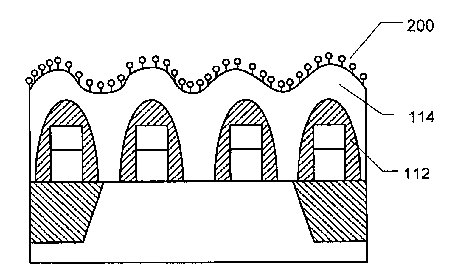
[0014] The exemplary embodiments of the present invention address the noted problems of the conventional CMP processes by providing new slurry compositions that are suitable for use in processes involving the chemical mechanical polishing (CMP) of a polysilicon layer to reduce or eliminate the excessive removal of the polysilicon layer.

Problems solved by technology

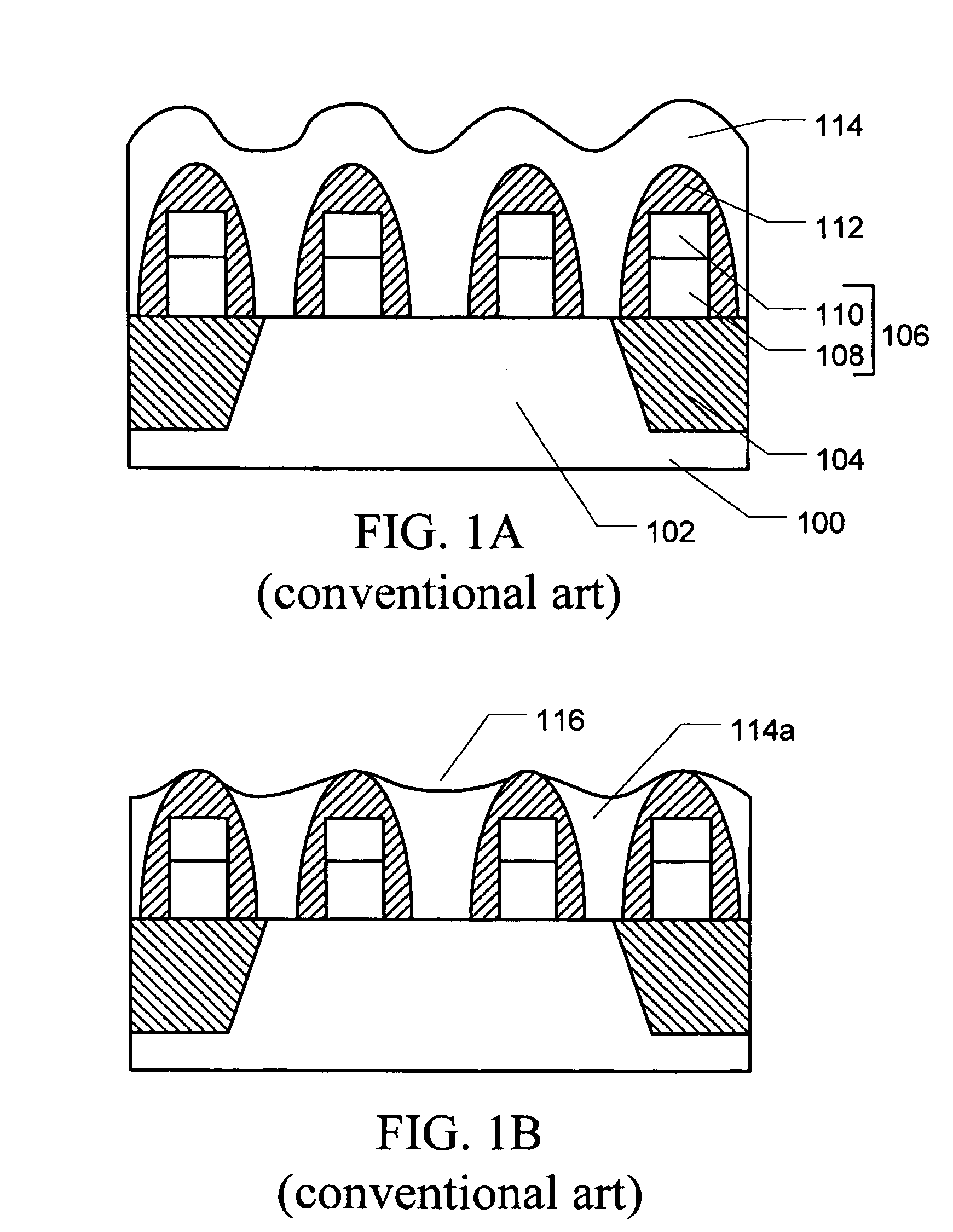
In certain instances, however, it may not be possible or practical to utilize a polishing stopping layer, or the relative characteristics of the materials being removed can tend to result in “dishing” or “cupping” of the more easily removed material and produces a more non-planar surface than desired and may compromise subsequent processing.
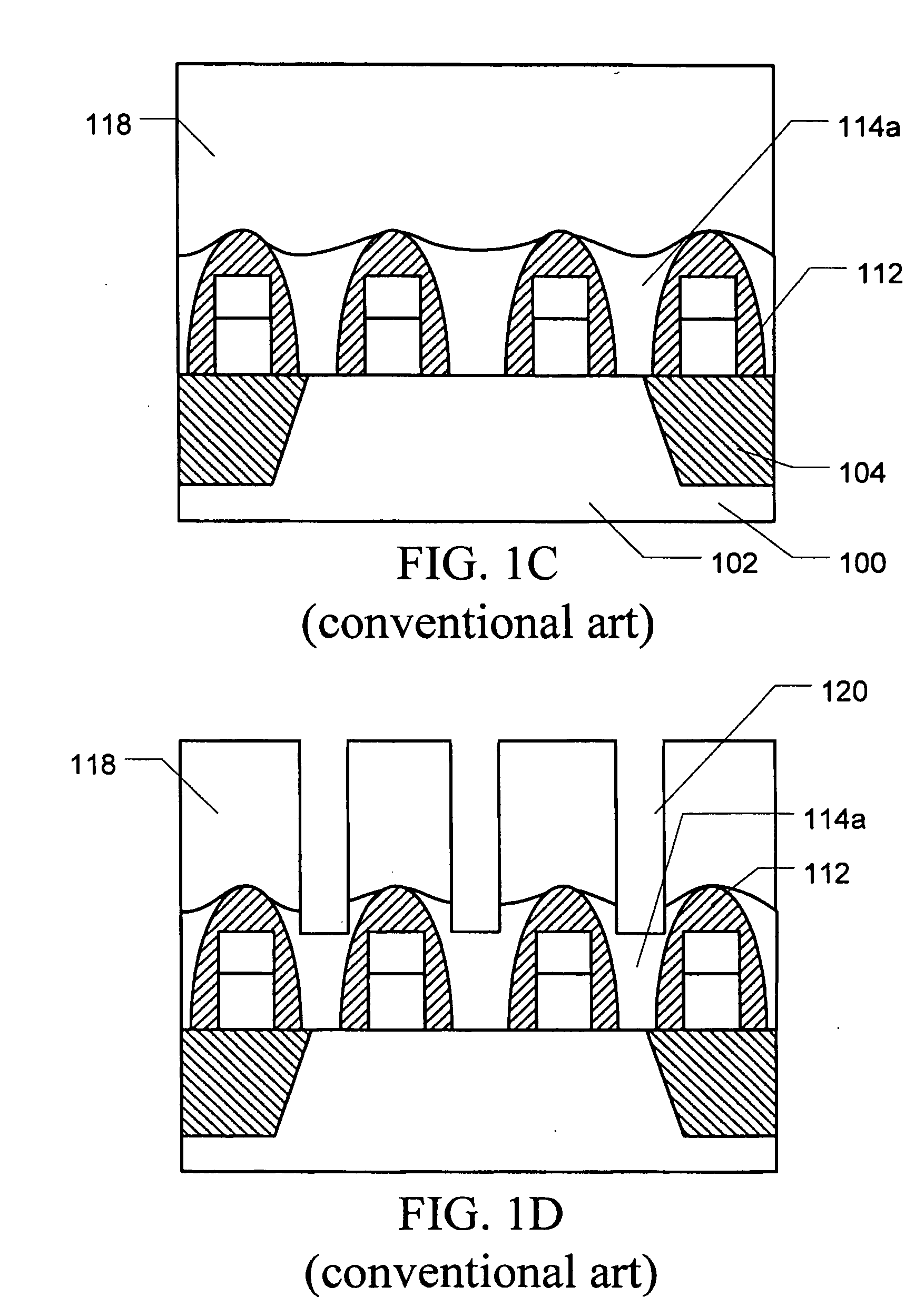
However, because polysilicon may be removed at a rate greater than the rate at which silicon oxide or silicon nitride are removed, in some instances as much as 50 to 100 times greater, there is a tendency for excessive polysilicon to be removed, forming depressions 116 between the spacer structures and produce a non-planar surface.
This increased thickness can result in problems such as the underetch condition illustrated in FIG. 1E wherein the etch is not sufficient to open some or all of the contact openings, leaving regions of residual ILD 118a in the bottom of the contact openings.
Similarly, as illustrated in FIG. 1F, in those instances in which the depth of the etch is sufficient to reach the polysilicon, but the contact pattern is misaligned, the contacts openings can expose the gate electrodes 106 or other conductive structures, causing shorts in region S. Both opens and shorts will reduce the process yield and / or reduce the reliability of the final semiconductor devices.

Method used


Image

  • Slurry compositions and CMP methods using the same
  • Slurry compositions and CMP methods using the same
  • Slurry compositions and CMP methods using the same

Examples


Embodiment Construction

[0023] Accordingly, the exemplary embodiments of the present invention comprise or incorporate a slurry composition for the chemical mechanical polishing of a polysilicon layer that includes at least a carrier liquid, abrasive particles, and a polymeric surfactant that includes both hydrophilic and hydrophobic functional groups. The polymeric surfactant will include at least one polymer alcohol including ethylene oxide (EO) and propylene oxide (PO), either as a copolymer or as a triblock polymer.

[0024] When used for polishing polysilicon, the hydrophobic functional groups of the polymeric surfactant attach preferentially to the exposed polysilicon surface, thereby forming a passivation layer. This passivation layer is sufficient to reduce the removal rate of the polysilicon layer relative to any exposed silicon oxide or silicon nitride surfaces and reduce or eliminate the excessive removal of polysilicon. The slurry composition may, of course, and preferably will include additional...


PUM


Abstract

The exemplary embodiments of the present invention providing new slurry compositions suitable for use in processes involving the chemical mechanical polishing (CMP) of a polysilicon layer. The slurry compositions include one or more non-ionic polymeric surfactants that will selectively form a passivation layer on an exposed polysilicon surface in order to suppress the polysilicon removal rate relative to silicon oxide and silicon nitride and improve the planarity of the polished substrate. Exemplary surfactants include alkyl and aryl alcohols of ethylene oxide (EO) and propylene oxide (PO) block copolymers and may be present in the slurry compositions in an amount of up to about 5 wt %, although much smaller concentrations may be effective. Other slurry additives may include viscosity modifiers, pH modifiers, dispersion agents, chelating agents, and amine or imine surfactants suitable for modifying the relative removal rates of silicon nitride and silicon oxide.

Description

CROSS-REFERENCE TO RELATED APPLICATION [0001] This application claims priority from Korean Patent Application No. 10-2003-0090551, which was filed on 12 Dec. 2003 in the Korean Intellectual Property Office, the disclosure of which is incorporated herein in its entirety by reference. BACKGROUND OF THE INVENTION [0002] 1. Field of the Invention [0003] The present invention relates to slurry compositions and methods using such slurry compositions for the chemical mechanical polishing (CMP) of material layers deposited during the manufacture of semiconductor devices, more particularly to slurry compositions including one or more additives for adjusting the relative removal rates of different materials, and most particularly to slurry compositions including one or more additives for reducing the removal rate of polysilicon relative to other materials present on a semiconductor substrate. [0004] 2. Description of the Related Art [0005] The increasing demand for high performance semiconduc...

Claims


Application Information

Patent Timeline
IPC IPC(8): C09G1/02H01L21/302H01L21/321H01L21/461H01L21/76H01L21/768
CPCC09G1/02H01L21/7684H01L21/3212C09K3/1463
Inventor CHOI, JAEKWANGLEE, JAEDONGHONG, CHANG-KI
Owner SAMSUNG ELECTRONICS CO LTD
Why Eureka
Eureka Blog
Learn More