
ESD protection design against charge-device model ESD events

a charge-device model and protection design technology, applied in the field of esd protection, can solve the problems of damage to the ic pin, damage to the chip,

Inactive Publication Date: 2005-06-09
TRANSPACIFIC IP LTD
View PDF18 Cites 7 Cited by
  • Summary
  • Abstract
  • Description
  • Claims
  • Application Information

AI Technical Summary

Benefits of technology

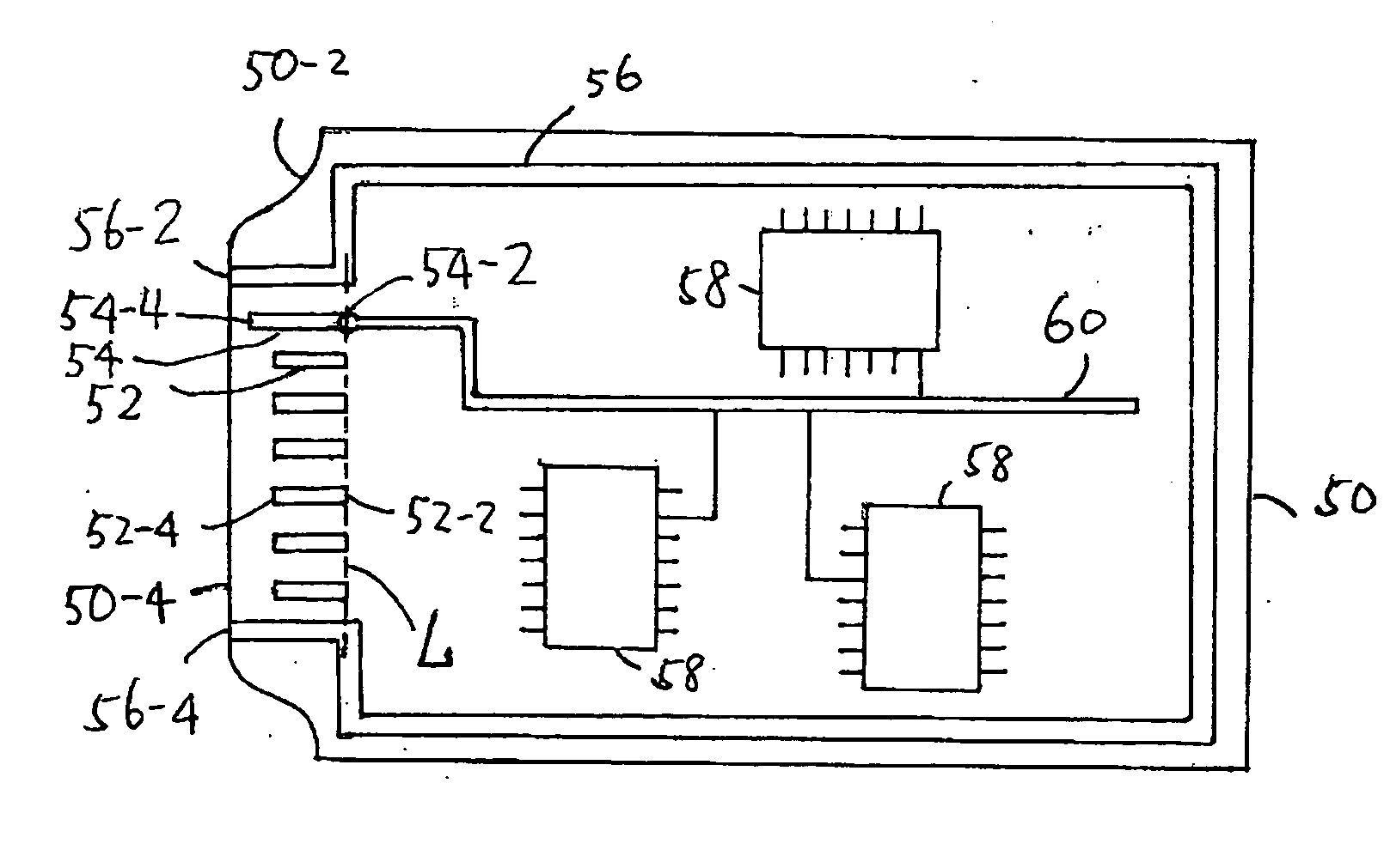
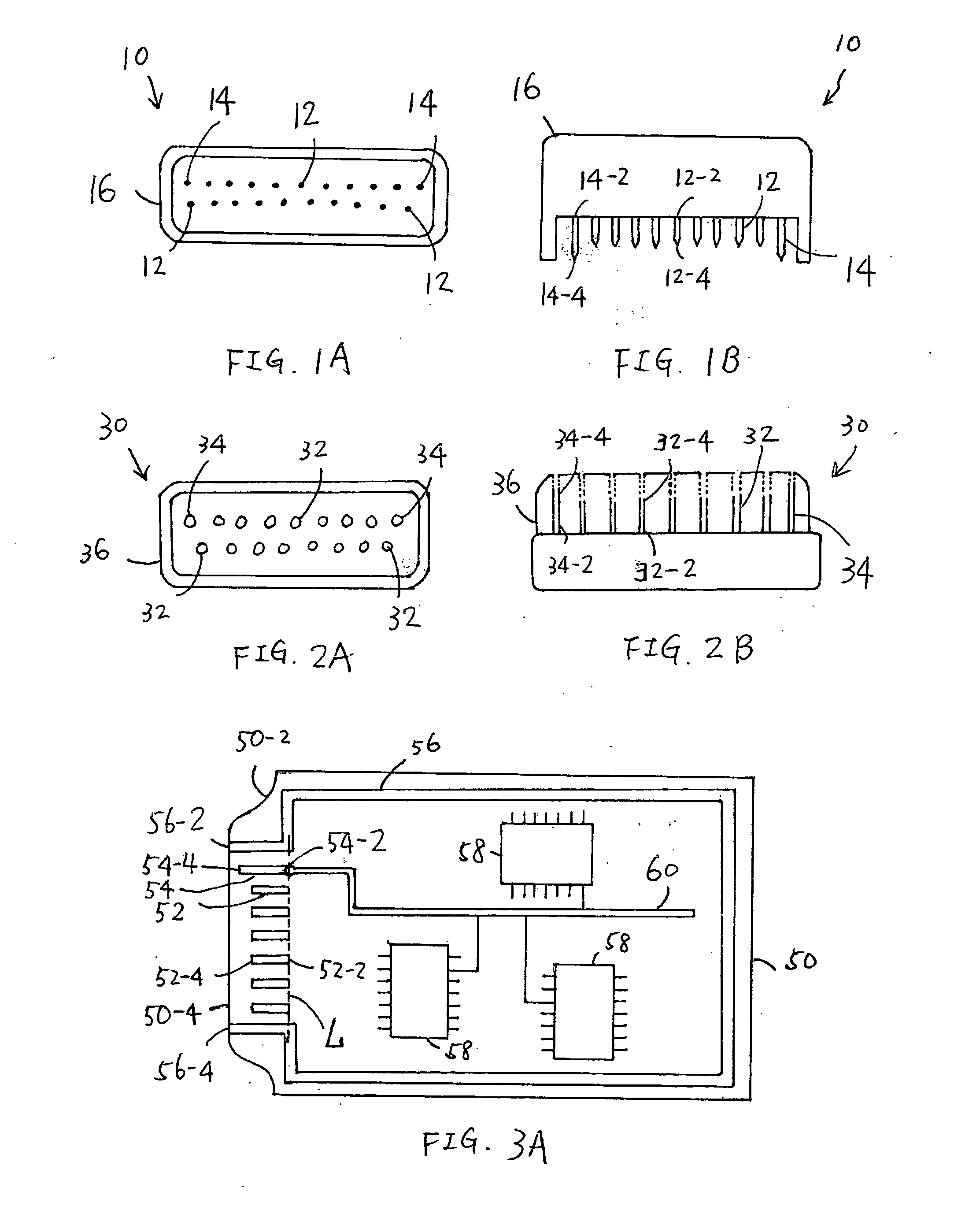
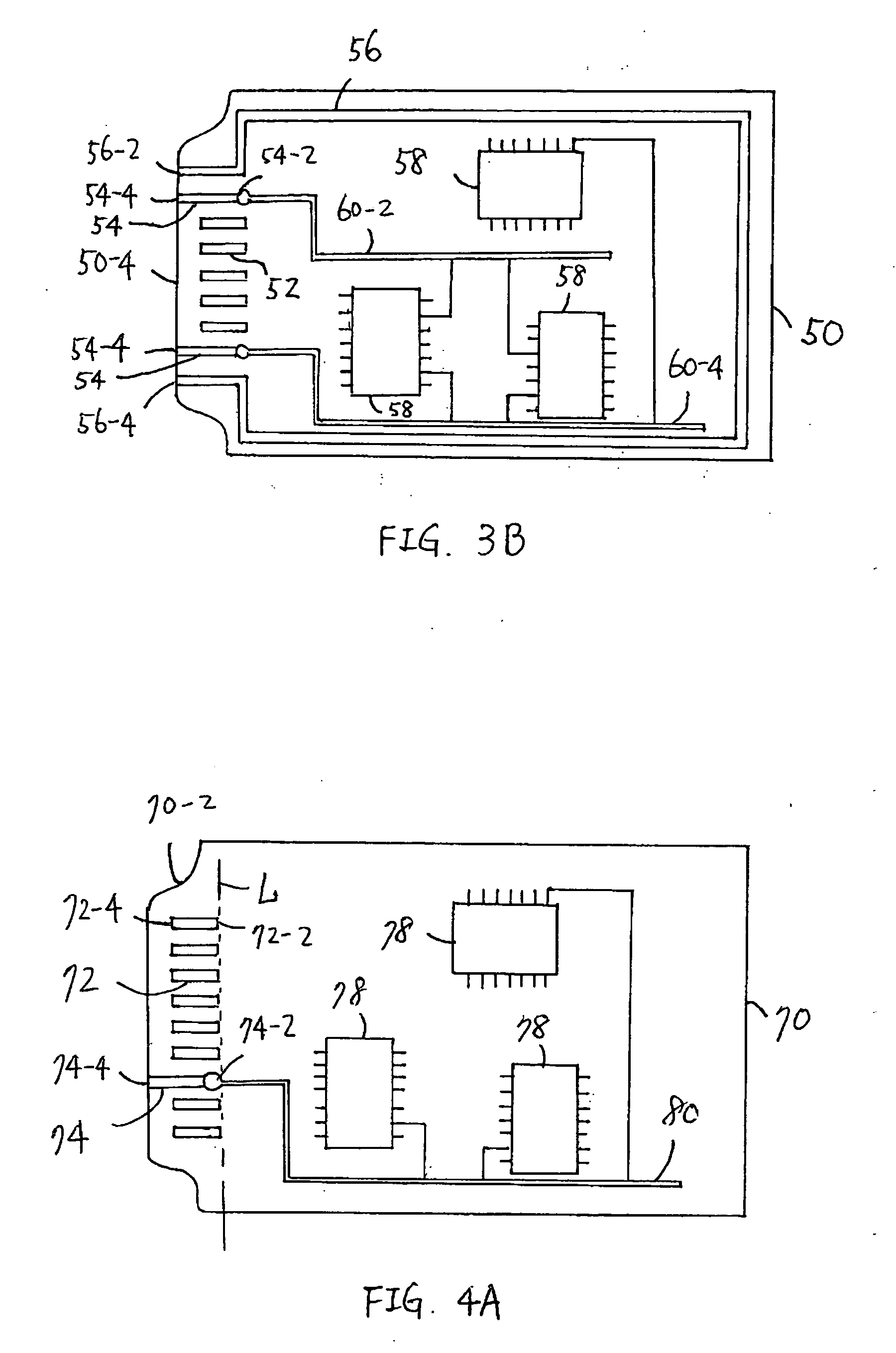
[0022] Still in accordance with the present invention, there is provided a method of providing electrostatic discharge protection for integrated circuits formed on a board that comprises forming a plurality of a first contact lines near a side of the board, providing each of the first contact lines with one end connected to the board and the other end to connect to an external device, forming at least one second contact line near the same side of the board corresponding to at least one voltage line of a voltage level to which the integrated circuits are connected, providing each of the at least one second contact line with one end connected to a corresponding voltage line and the other end connected to the external device, providing the other end of each of the at least one second contact line closer to an edge on the side of the board than the other end of each of the first contact lines, coupling the board to the external device, and discharging electric charges accumulated on the board via the at least one second contact line.

Problems solved by technology

A semiconductor integrated circuit (“IC”) is generally susceptible to an electrostatic discharge (“ESD”) event, which may damage or destroy the IC.
The above-mentioned ESD protection schemes, however, are designed to increase ESD immunity of individual chips, and may not provide sufficient protection for the chips under a board-level CDM ESD event.
Since the capacitance of the board is much greater than that of the ICs, the board-level CDM ESD event may occur when electric charges accumulated on the board are discharged to ground through pins of the ICs, resulting in damage to the IC pins.
The above-mentioned ESD protection techniques for connectors or PCBs, however, are designed to increase ESD immunity of a system against an HBM-like ESD event, and may not provide sufficient protection for the chips under a board-level CDM ESD event.

Method used


Image

  • ESD protection design against charge-device model ESD events
  • ESD protection design against charge-device model ESD events
  • ESD protection design against charge-device model ESD events

Examples


Embodiment Construction

[0001] 1. Field of the Invention

[0002] This invention pertains in general to circuits and methods for electrostatic discharge (“ESD”) protection and, more particularly, to circuits and methods for a charged-device model (“CDM”) ESD protection.

[0003] 2. Background of the Invention

[0004] A semiconductor integrated circuit (“IC”) is generally susceptible to an electrostatic discharge (“ESD”) event, which may damage or destroy the IC. An ESD event refers to a phenomenon of electrical discharge of a current (positive or negative) for a short duration during which a large amount of current is provided to the IC. The susceptibility of a device to ESD can be determined by testing for one of three models, Human Body Model (HBM), Machines Model (MM), and Charged-Device Model (CDM).

[0005] The ESD Association Standard for the Development of an Electrostatic Discharge Control Program for Protection of Electrical and Electronic Parts, Assemblies and Equipment (Excluding Electrically Initiated...


PUM


Abstract

An interface device coupled to a board on which integrated circuits are mounted for providing electrostatic discharge protection for the integrated circuits that comprises a plurality of first contact members, each of the first contact members including one end connected to the board and the other end to connect to an external device, and at least one second contact member connected to a voltage line of a voltage level, wherein the at least one second contact member includes a length greater than that of each of the first contact members.

Description

DESCRIPTION OF THE INVENTION [0001] 1. Field of the Invention [0002] This invention pertains in general to circuits and methods for electrostatic discharge (“ESD”) protection and, more particularly, to circuits and methods for a charged-device model (“CDM”) ESD protection. [0003] 2. Background of the Invention [0004] A semiconductor integrated circuit (“IC”) is generally susceptible to an electrostatic discharge (“ESD”) event, which may damage or destroy the IC. An ESD event refers to a phenomenon of electrical discharge of a current (positive or negative) for a short duration during which a large amount of current is provided to the IC. The susceptibility of a device to ESD can be determined by testing for one of three models, Human Body Model (HBM), Machines Model (MM), and Charged-Device Model (CDM). [0005] The ESD Association Standard for the Development of an Electrostatic Discharge Control Program for Protection of Electrical and Electronic Parts, Assemblies and Equipment (Exc...

Claims


Application Information

Patent Timeline
IPC IPC(8): H05K1/02H05K1/11H05K9/00
CPCH05K1/0259H05K1/117H05K2201/10689H05K2201/09354H05K2201/094H05K9/0067
Inventor KER, MING-DOULIN, KUN-HSIEN
Owner TRANSPACIFIC IP LTD
Learn More