Method of manufacturing split-gate memory

a technology of split-gate memory and manufacturing method, which is applied in the direction of semiconductor devices, electrical devices, transistors, etc., can solve the problems of reducing the erasure operation properties of flash memory devices, and achieve the enhancement the improvement of the erasure efficiency of the present invention

Active Publication Date: 2005-05-26
SAMSUNG ELECTRONICS CO LTD
View PDF5 Cites 16 Cited by
  • Summary
  • Abstract
  • Description
  • Claims
  • Application Information

AI Technical Summary

Benefits of technology

[0022] The present invention provides a method of manufacturing a split-gate flash memory having improved erasure efficiency. In one aspect, erasure efficiency associated with the present invention is enhanced by forming a high voltage gate insulating film and a tunneling insulating film having different thicknesses. In a related aspect, stable erasure voltage, as applied to the control gate of a flash memory device formed in accordance with the present invention, is ensured by the formation of a high voltage gate insulating film having a sufficient thickness.

Problems solved by technology

As a result, the erasure operation properties of the flash memory device degrade accordingly.

Method used


Image

  • Method of manufacturing split-gate memory
  • Method of manufacturing split-gate memory
  • Method of manufacturing split-gate memory

Examples


Embodiment Construction

[0035] The present invention will now be described in some additional detail with reference to the accompanying drawings. The invention may, however, be embodied in many different forms and should not be construed as being limited to only the embodiments set forth herein. Rather, these embodiments are presently preferred teaching examples. Those of ordinary skill in the art will recognize that various modifications and alterations to the illustrated embodiments are possible. Further, those of ordinary skill understand that when an element such as a layer, region or substrate is referred to as being “on” or “onto” another element, the layer may be either directly on the other element or intervening elements may also be present.

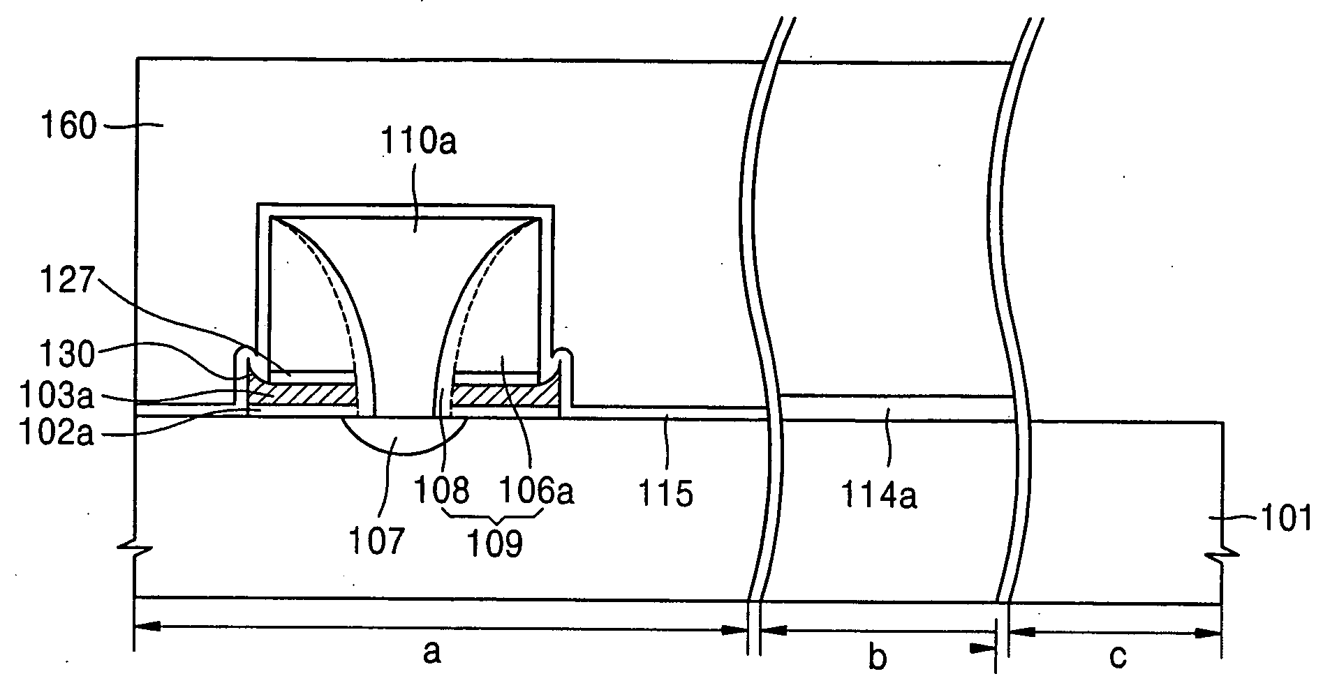
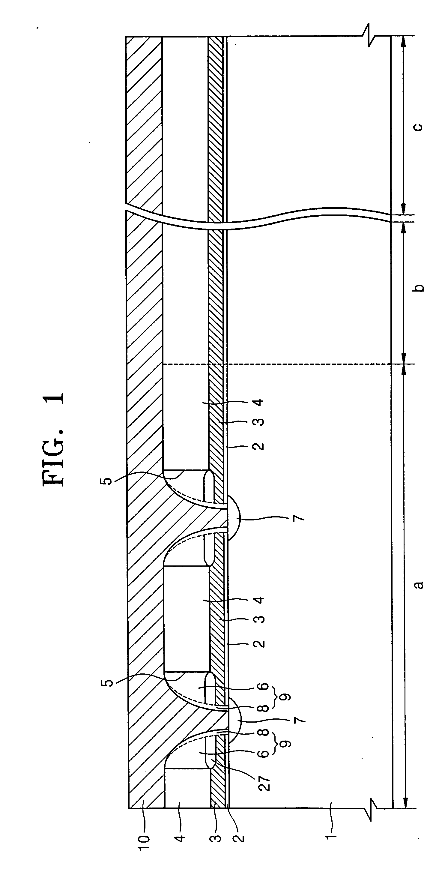
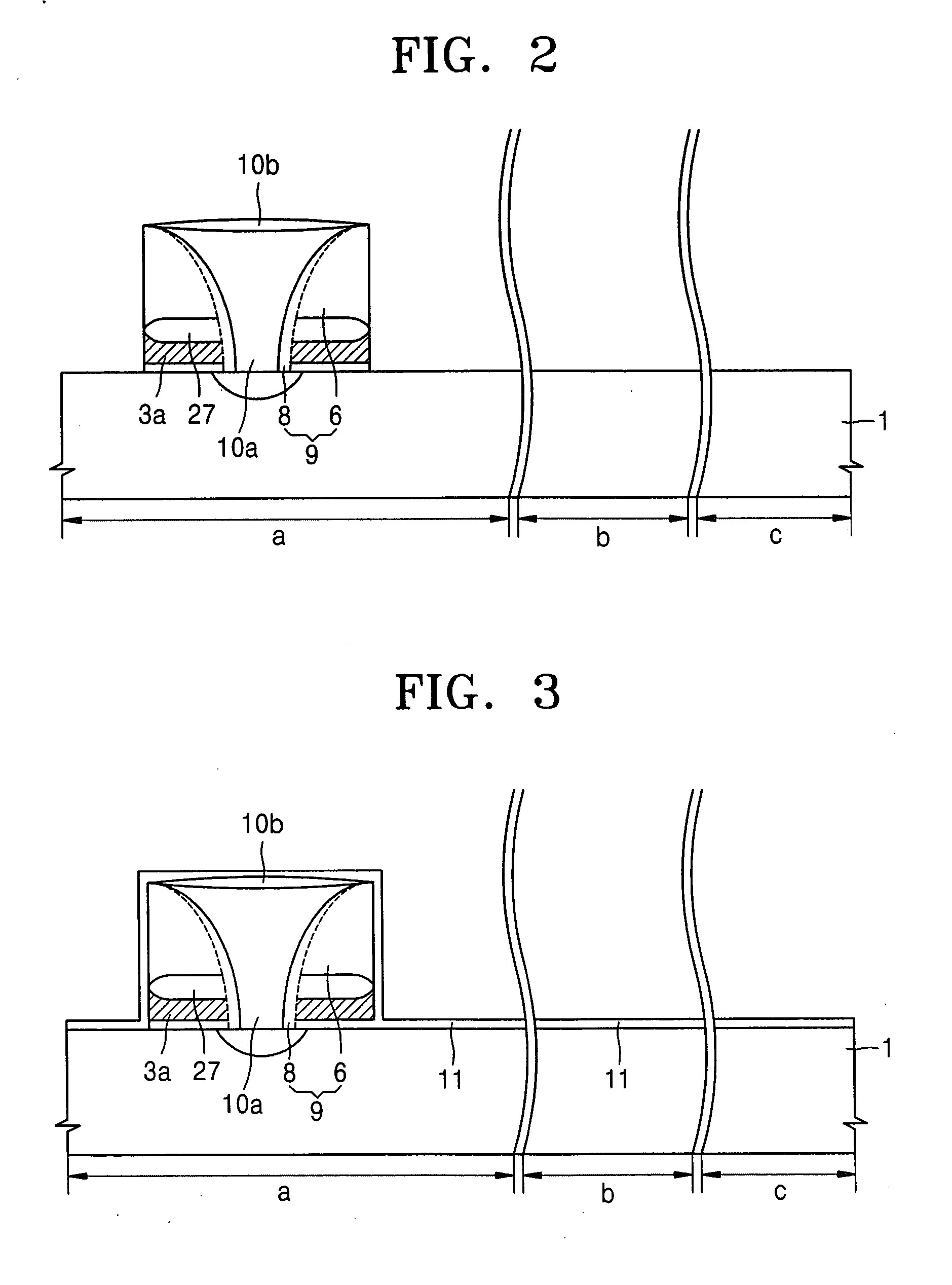
[0036]FIGS. 10 through 26 are cross-sectional views illustrating a method of manufacturing a split-gate flash memory according to one embodiment of the present invention. Referring to FIG. 10, a coupling insulating film 102, a floating gate conductive film 103...


PUM


Abstract

A method of manufacturing split-gate memory provides a control gate insulating film and the tunneling insulating film in a cell region, a high voltage gate insulating film in a high voltage region, and a low voltage gate insulating film in a low voltage region, all having different thickness. Additionally, a pre-cleaning process removes an outer sidewall portion of a spacer to form a tip portion of a floating gate that overlaps a control gate line formed proximate the floating gate.

Description

BACKGROUND OF THE INVENTION [0001] 1. Field of the Invention [0002] The present invention relates to a method of manufacturing a non-volatile memory. More particularly, the present invention relates to a method of manufacturing a split-gate flash memory having a cell region and peripheral circuit regions. [0003] A claim of priority is made to Korean Patent Application No. 2003-84733 filed on Nov. 26, 2003, the disclosure of which is incorporated herein by reference in its entirety. [0004] 2. Description of the Related Art [0005] A non-volatile memory maintains data stored in its constituent memory cells even in those circumstances where power is not applied to the memory. Examples of non-volatile memory types include; mask ROMs, erasable and programmable ROMs (EPROMs), and an electrically erasable and programmable ROM (EEPROMs). Flash memory is one form of EEPROM in which one transistor constitutes one memory cell. [0006] Different flash memory types include the stacked gate flash m...

Claims


Application Information

Patent Timeline
Patent Type & Authority Applications(United States)
IPC IPC(8): H01L21/28H01L21/336H01L21/8247H01L27/115H01L29/788H01L29/792
CPCH01L21/28273H01L27/11521H01L29/66825H01L27/11536H01L29/66553H01L27/11526H01L29/40114H10B41/44H10B41/40H10B41/30H10B99/00
Inventor KIM, YONG-HEEKWON, CHUL-SOONKIMKIM, JOO-CHANKIM, DAE-GEUNRYU, EUI-YOUL
Owner SAMSUNG ELECTRONICS CO LTD
Why Eureka
Try Eureka