Semiconductor device with multi-bank DRAM and cache memory

a multi-bank, cache memory technology, applied in the direction of memory adressing/allocation/relocation, digital storage, instruments, etc., can solve the problems of mounting space, no refresh operation, and complicated and troublesome control of the dram

Inactive Publication Date: 2005-05-26
RENESAS TECH CORP
View PDF10 Cites 5 Cited by
  • Summary
  • Abstract
  • Description
  • Claims
  • Application Information

AI Technical Summary

Benefits of technology

[0008] Under such circumstances, it is an object of the present invention to provide a memory device that can solve the above problems.
[0009] According to one aspect of the present invention, the memory device composed of a DRAM consisting of a cache memory and a plurality of banks is constituted such that: each cache line of a cache memory in a memory device is divided into sub lines; and there is provided each sub line with a valid bit and a dirty bit so as to hide refresh operations. This makes it possible to execute only a write-back operation for the DRAM array when a write access to a sub line in which the dirty bit is set is decided as a cache miss.
[0010] At the same time, the valid bit of each sub line other than the accessed one is reset to invalidate their data, thereby eliminating the allocate operation from the DRAM array. This can prevents two banks from being kept accessed.
[0012] Consequently, the above conventional problem is solved; concretely, even when consecutive write accesses to the same cache line are decided as cache misses, the DRAM array can be driven into the idle state in which no access is done, thereby the refresh operation can be executed therein.
[0013] The effects of the present invention is to realize a memory with excellent operability without causing the refresh operation in the DRAM array to delay external accesses, in other words, to realize a memory compatible with an SRAM in which refresh operations can be hidden from external.

Problems solved by technology

In spite of this, the SRAM, since it is composed of six transistors, requires a large space for disposing memory cells, encountering a problem of mounting space when it employed to be mounted on an LSI together with other parts.
The DRAM, however, has disadvantages in which its cycle time is slower than that of the SRAM and the DRAM is required to be refreshed, causing it rather complicated and troublesome to control the DRAM.
In other words, no refresh operation can be done in those two banks, thereby some data in the DRAM might be damaged.

Method used


Image

  • Semiconductor device with multi-bank DRAM and cache memory
  • Semiconductor device with multi-bank DRAM and cache memory
  • Semiconductor device with multi-bank DRAM and cache memory

Examples


first embodiment

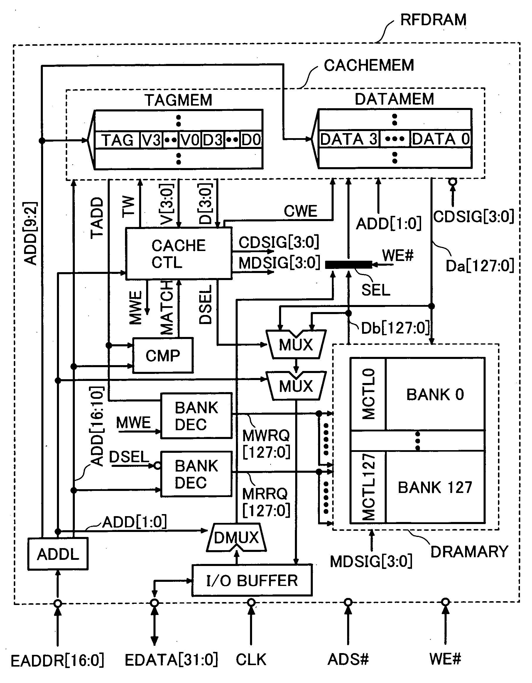
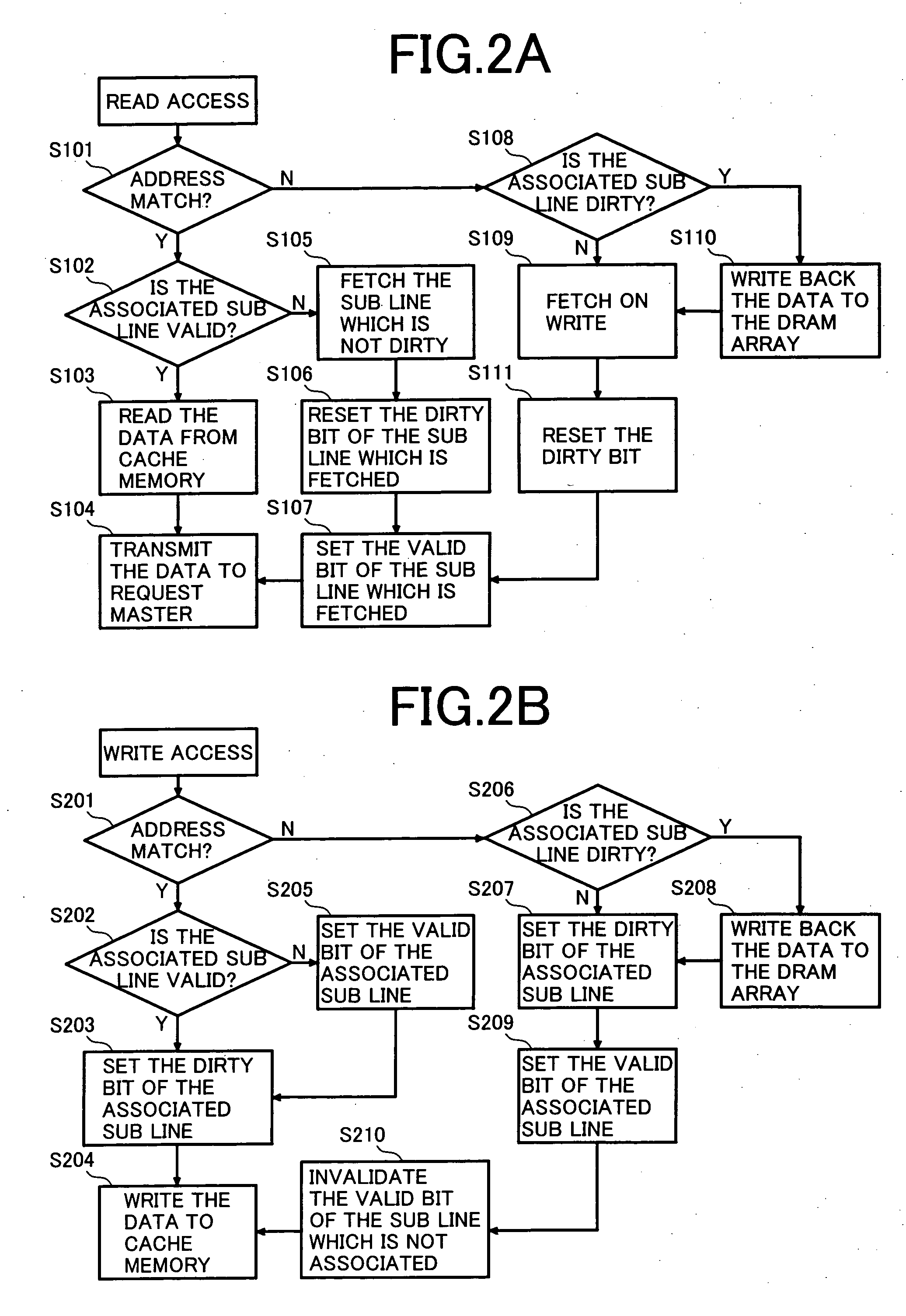
[0026]FIG. 1 shows a block diagram of a refresh free dynamic memory RFDRAM (referred to as RFDRAM hereinafter), which is a memory device in an embodiment of the present invention. FIG. 2 shows a flowchart of the operation of the RFDRAM. FIG. 3A and 3B show embodiments of a cache memory and FIGS. 4A and 4B show embodiments of a DRAM memory array used in the RFDRAM shown in FIG. 1. FIG. 5 shows a timing chart of the RFDRAM denoting that it is possible to avoid a confliction between an access and a refresh operation requested to the DRAM array concurrently.

[0027] As shown in FIG. 1, the RFDRAM is composed of a cache memory CACHEMEM and a DRAM array DRAMARY, which consists of a plurality of DRAM banks (128 banks (bank 127 to bank 0)) In the example shown in FIG. 1, the capacity of one bank is 32k bits and the total capacity of the memory is 4M bits. The capacity of the cache memory CACHEMEM is equivalent to that of one bank. In FIG. 1, the cache memory consists of 16-byte wide cache li...

second embodiment

[0073]FIG. 6 shows the second embodiment of the RFDRAM of the present invention. The cache memory in this embodiment is controlled by the direct mapped caching scheme. The main difference from the first embodiment is that the external data bus EDATA[127:0] and the internal data bus Da[127:0] / Db[127:0] is equal in data width. In other words, the data width is the same among the data input / output to / from the DRAM array DRAMARY, the cache line, and the external data bus EDATA[127:0]. This configuration can eliminate dividing of a cache line into sub lines, so that the tag memory TAGMEM requires only a valid bit and a dirty bit. In addition, because the minimum unit of data management is equal to the data width of the cache line, the cache data control signal CDSIG[3:0] and the memory data control signal MDSIG[3:0] can be omitted. The address match signal MATCH is used instead of the data select signal DSEL that is inputted to the multiplexer MUX.

[0074] The memory operation in the seco...

third embodiment

[0083]FIG. 7 shows the third embodiment of the RFDRAM of the present invention. The main difference from the first and second embodiments is that the cache memory CACHEMEM is composed of a plurality of tag memories TAGMEMa and TAGMEMb, as well as a plurality of data memories DATAMEMa and DATAMEMb and the set associative method is employed to control the cache memory CACHEMEM in this embodiment. The cache hit decision method in this embodiment also differs from that in other embodiments. In addition, the RFDRAM is provided with a write buffer WBUFFER, a write back buffer WBB, a hit way signal HITWAY, a way selector signal WAYSEL, and a write tag address bus WTADD, etc.

[0084] On the other hand, there in no need to divide a cache line into sub lines in this third embodiment, so that the cache data control signal CDSIG[3:0] and the memory data control signal MDSIG[3:0] are omitted just like in the second embodiment. Just like in the second embodiment, each cache line is provided with a...


PUM


Abstract

To provide means that can hide refresh operations even when the data width of a cache line differs from that of the external data bus in a memory that uses a cache memory and a DRAM consisting of a plurality of banks. A semiconductor device consisting of a plurality of memory banks BANK0 to BANK127, each consisting of a plurality of memory cells, as well as a cache memory CACHEMEM used to retain information read from the plurality of memory banks. The cache memory CACHEMEM consists of a plurality of entries, each having a data memory DATAMEM and a tag memory TAGMEM. The data memory DATAMEM consists of a plurality of sub lines DATA0 to DATA3 and the tag memory TAGMEM Consists of a plurality of valid bits V0 to V3 and a plurality of dirty bits D0 to D3. It is possible to realize a memory with excellent operability, causing no refresh operation to delay external accesses. In other words, it is possible to realize a memory compatible with an SRAM in which refresh operations are hidden from external.

Description

FIELD OF THE INVENTION [0001] The present invention relates to a semiconductor device with a multi-bank DRAM and a cache memory. More particularly, the invention relates to a semiconductor device with a multi-bank DRAM and a cache memory, preferably used for fast, highly integrated, and low power consumption apparatuses. The invention also relates to a semiconductor device with a multi-bank DRAM and a cache memory, in which logical circuits and semiconductor memory devices are integrated. BACKGROUND OF THE INVENTION [0002] The static random access memory (referred to as SRAM hereinafter) is the main stream of the on-chip memories to be mounted on an LSI together with other parts. In spite of this, the SRAM, since it is composed of six transistors, requires a large space for disposing memory cells, encountering a problem of mounting space when it employed to be mounted on an LSI together with other parts. [0003] There is another method where a dynamic random access memory (referred t...

Claims


Application Information

Patent Timeline
Patent Type & Authority Applications(United States)
IPC IPC(8): G06F12/08G11C11/401G11C11/403G11C11/406G11C11/41
CPCG06F12/0893G06F2212/3042G11C2207/2245G11C11/40615G11C11/406
Inventor AKIYAMA, SATORUKANNO, YUSUKEWATANABE, TAKAO
Owner RENESAS TECH CORP
Why Eureka
Try Eureka