
Refresh for dynamic cells with weak retention

a dynamic cell and weak retention technology, applied in static storage, digital storage, instruments, etc., can solve the problems of circuitry required to support redundancy, occupying a significant amount of chip area, and cell failures that have fallen below even the less stringent minimum retention time for normal parts

Inactive Publication Date: 2005-05-12
POLARIS INNOVATIONS LTD
View PDF5 Cites 87 Cited by
  • Summary
  • Abstract
  • Description
  • Claims
  • Application Information

AI Technical Summary

Benefits of technology

[0009] Embodiments of the present invention generally provide improved methods and circuit configurations for utilizing memory cells having weak retention times.

Problems solved by technology

Variables in the manufacturing process may result in a broad distribution of retention times for cells within a DRAM device.
However, cells that have fallen below even the less stringent minimum retention time for normal parts may be considered as having failed.
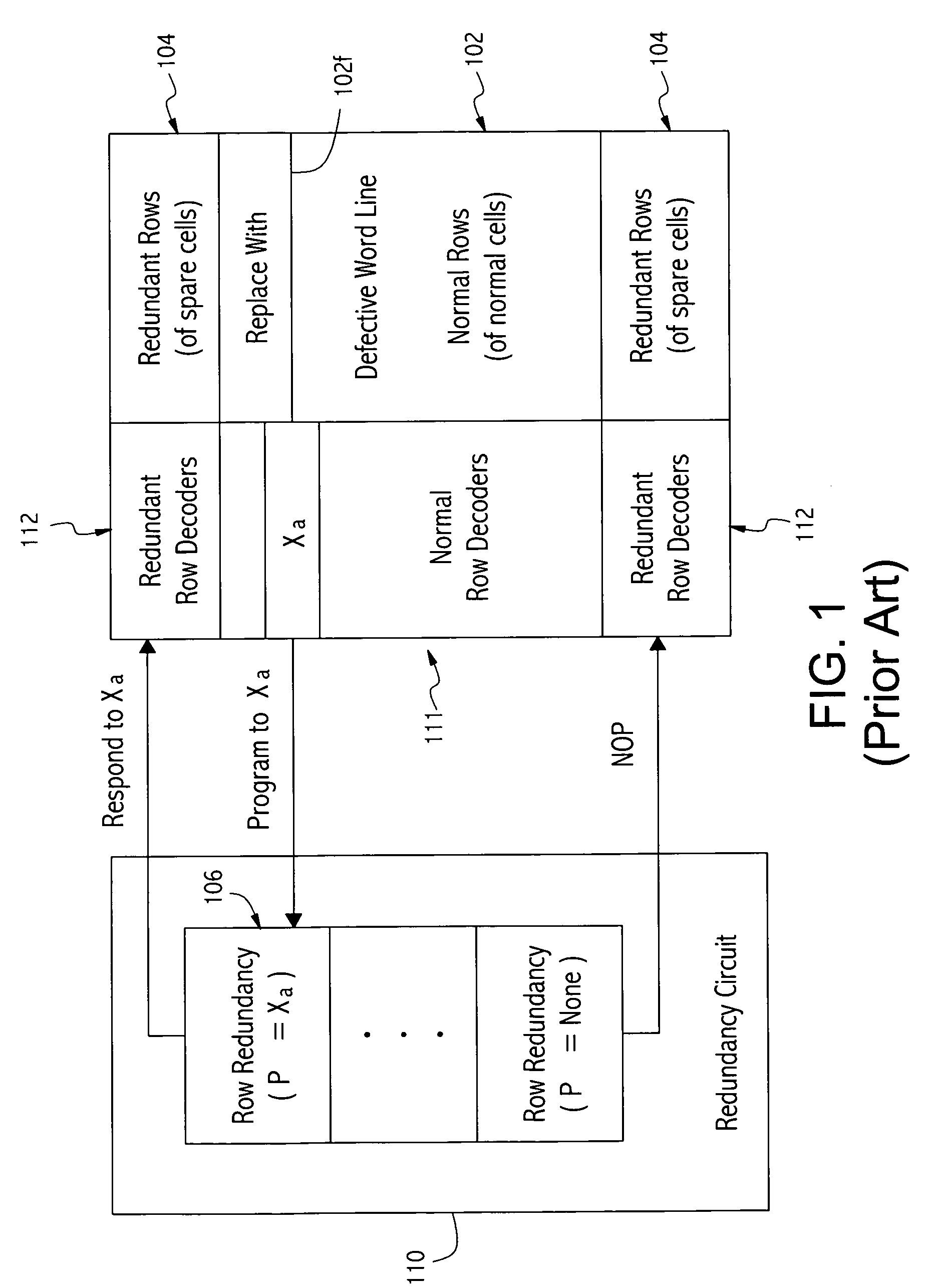
One disadvantage to this redundancy scheme, however, is that the circuitry required to support redundancy (e.g., the redundant rows themselves, the PROM registers, redundant row decoder, and comparison circuitry) occupies a significant amount of chip area, which increases with the number of redundant rows.
As a result, only a limited number of redundant rows are typically provided.

Method used


Image

  • Refresh for dynamic cells with weak retention
  • Refresh for dynamic cells with weak retention
  • Refresh for dynamic cells with weak retention

Examples


Embodiment Construction

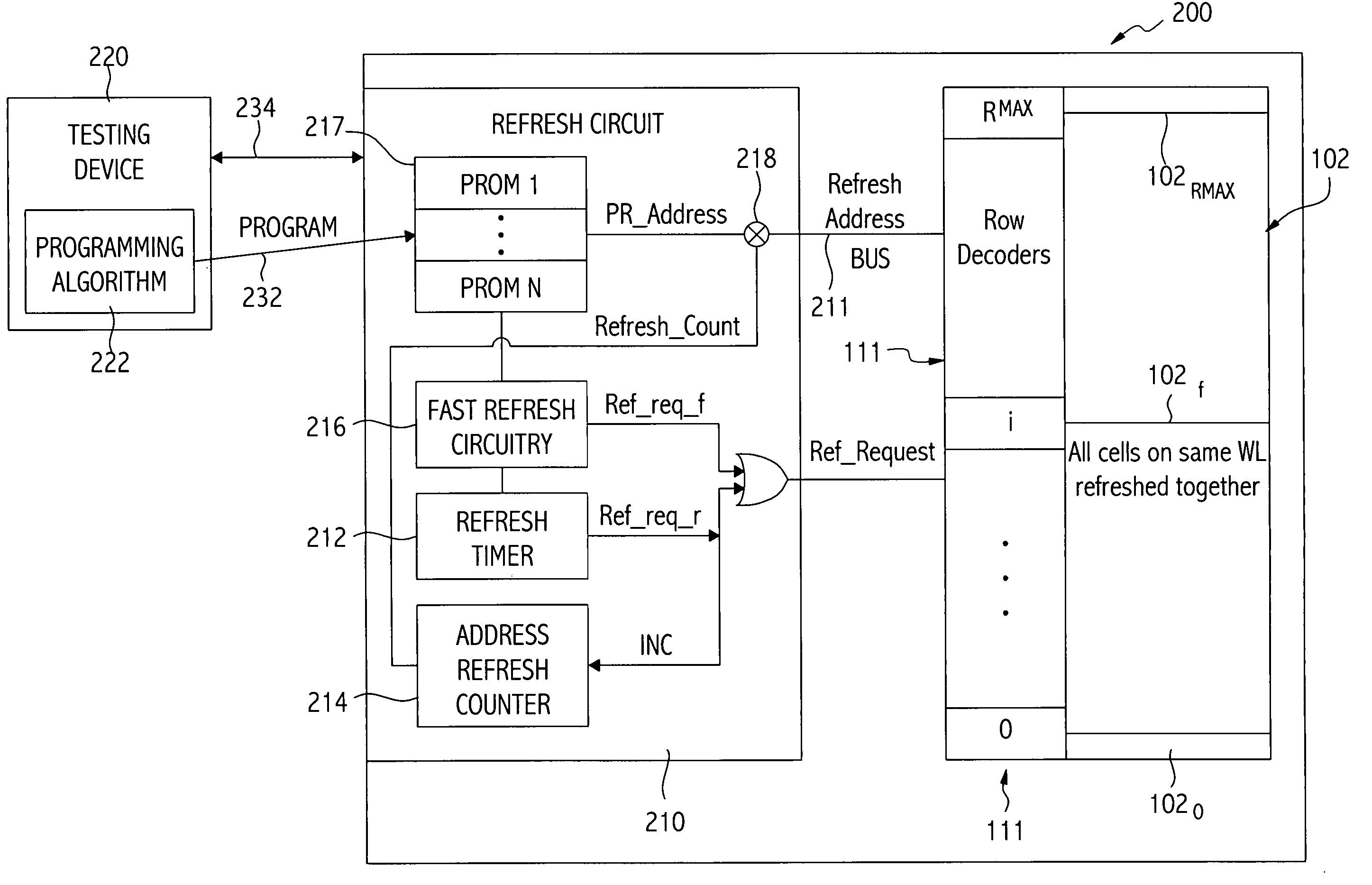
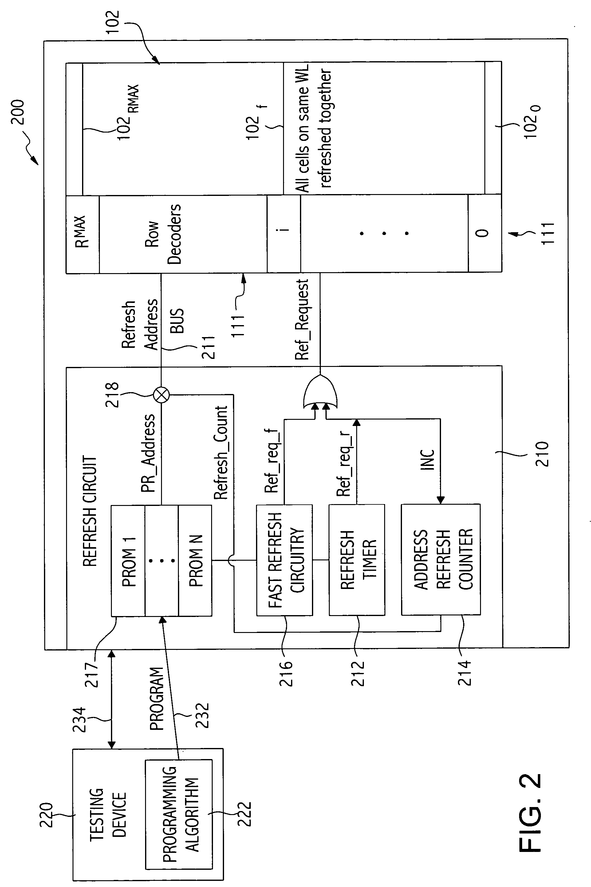
[0030] Embodiments of the present invention generally provide methods and circuit configurations for utilizing memory cells having weak retention times. For some embodiments, rows identified as having weak retention cells may be refreshed more often than “normal retention” cells. As an example, if a normal refresh period is TREF, weak retention cells may be refreshed every TREF / 2 or TREF / 4 (possibly depending on the actual measured retention time). As a result, weak retention cells may work properly at this increased refresh frequency, without being replaced by redundancy. While some cells may still fail (e.g., regardless of retention time), embodiments of the present invention may reduce chip area overhead by reducing the number of redundant circuits conventionally required to replace rows with weak retention cells.

[0031] The techniques and circuits described herein for refreshing weak retention cells may be used to advantage in any type of devices that utilize dynamic memory cell...


PUM


Abstract

Methods and circuit configurations for utilizing memory cells having weak retention times are provided. For some embodiments, rows identified as having weak retention cells may be refreshed more often than “normal retention” cells. As an example, if a normal refresh period is TREF, weak retention cells may be refreshed every TREF / 2 or TREF / 4 (possibly depending on the actual measured retention time).

Description

BACKGROUND OF THE INVENTION [0001] 1. Field of the Invention [0002] The present invention generally relates to semiconductor memory devices and, more particularly, to volatile semiconductor memory devices. [0003] 2. Description of the Related Art [0004] The evolution of sub-micron CMOS technology has resulted in an increasing demand for high-speed semiconductor memory devices, such as dynamic random access memory (DRAM) devices, pseudo static random access memory (PSRAM) devices, and the like. Herein, such memory devices are collectively referred to as DRAM devices. Such devices utilize memory cells consisting of one transistor and one capacitor. Due to leakage, the memory cells require periodic refreshing to protect data that is stored in the memory cell from corruption or decaying over time. The data stored in the memory cell is automatically restored to a full logic level when accessed (e.g., via a read or write operation), but must be periodically refreshed when not accessed. Th...

Claims


Application Information

Patent Timeline
Patent Type & Authority Applications(United States)
IPC IPC(8): G11C11/406G11C29/00G11C29/50
CPCG11C11/401G11C11/406G11C11/40622G11C2211/4067G11C29/50016G11C2211/4061G11C29/50
Inventor OH, JONG-HOON
Owner POLARIS INNOVATIONS LTD
Learn More