Integrated line driver
- Summary
- Abstract
- Description
- Claims
- Application Information
AI Technical Summary
Benefits of technology
Problems solved by technology
Method used
Image
Examples
first embodiment
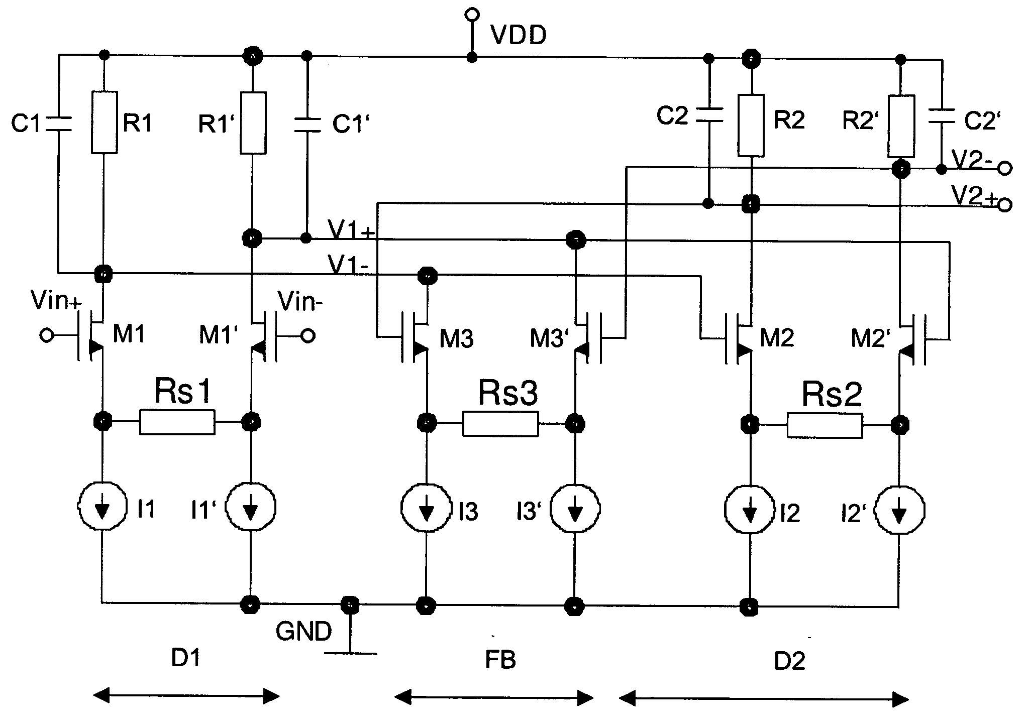
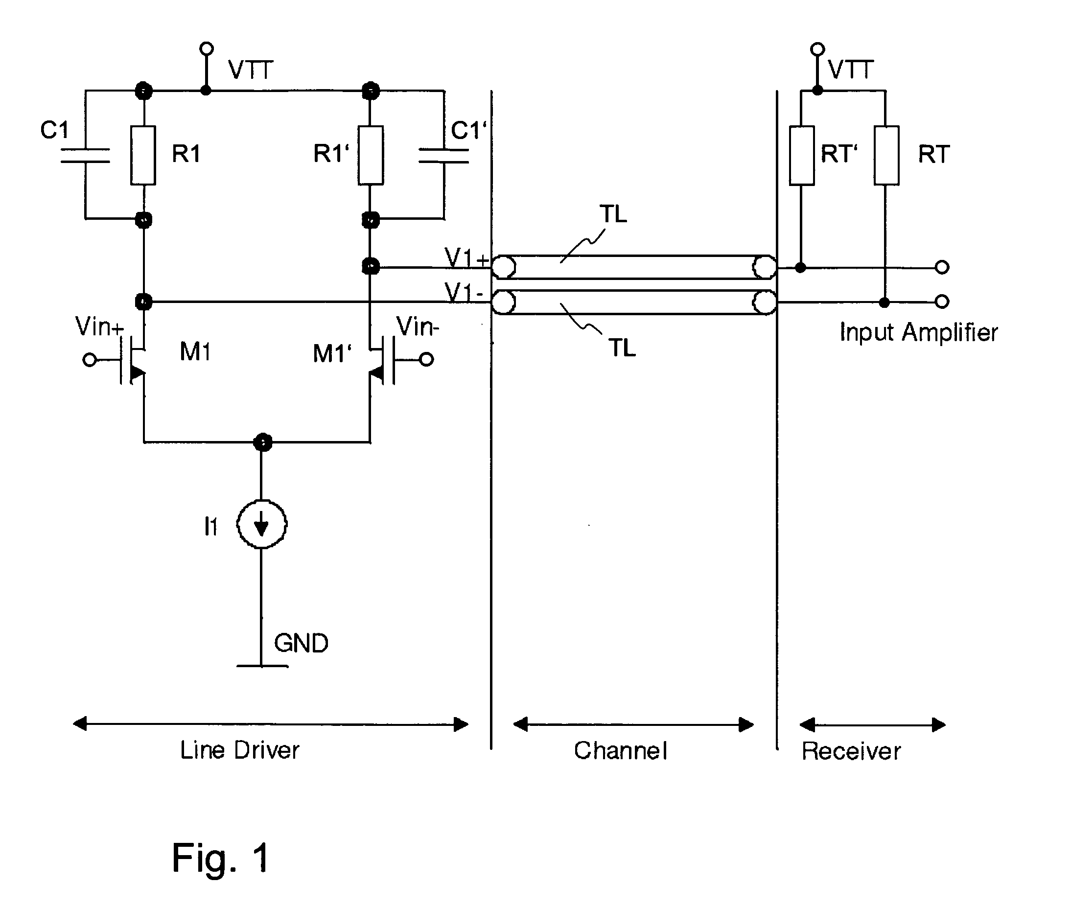
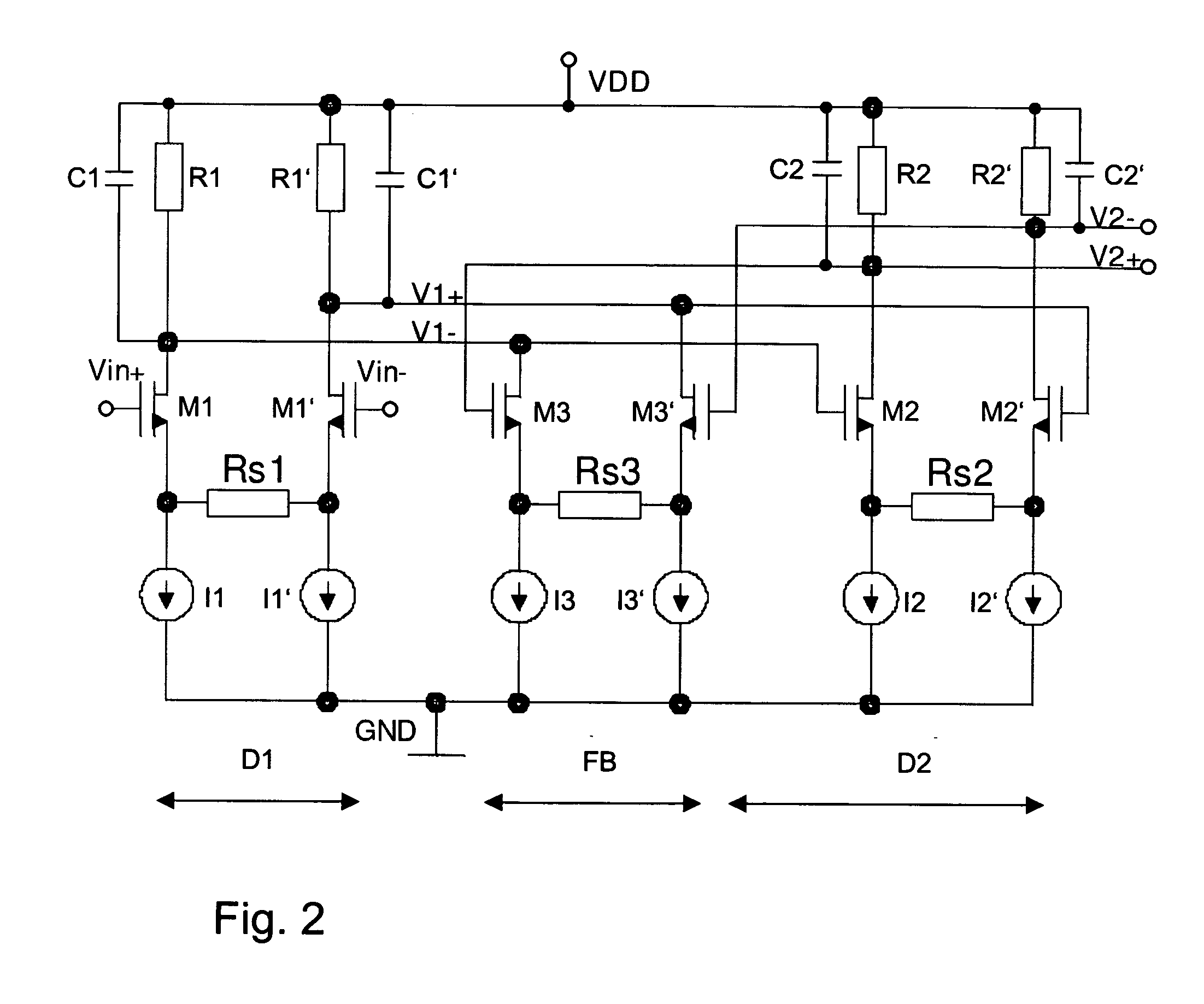
[0051] The design of the novel integrated line driver is illustrated in FIG. 2. The concept of the novel line driver is proposed in order to overcome the limitations of the conventional implementation of the line driver shown in FIG. 1 and the implementations mentioned in the section “Background of the invention”.
[0052] The first embodiment of the integrated line driver according to the invention comprises a first driver stage D1, shown on the left side of FIG. 2, a second driver stage D2, shown on the right side of FIG. 2, and a feedback device FB, shown in the middle of FIG. 2. The first embodiment of the integrated line driver is a line driver with active feedback.
[0053] The first driver stage D1 includes a first transistor M1 whose control input is connected to the input tap Vin+ of the first driver stage D1. Furthermore, it includes a further transistor M1′ whose control input is connected to the input tap Vin− of the first driver stage D1. Both transistors M1 and M1′ are inte...
second embodiment
[0073] In the embodiment depicted in FIG. 3 the feedback circuit FB comprises two resistors R3 and R3′ instead of the two transistors M3 and M3′. This second embodiment of the integrated line driver is a line driver with a passive feedback.
[0074] The DC gain k1 of the first driver stage D1 can be calculated to: k1=-gm1Rp11+(gm2-G3)·Rp2G3Rp1
wherein Rp1 is the parallel combination of the resistors R1 and R3.
[0075] The DC gain k2 of the first and second driver stage D1 and D2 can be calculated to: k2=gm1Rp1·(gm2-G3)Rp21+(gm2-G3)Rp2G3Rp1
[0076] The DC-loop gain k3 can be calculated to: k3=11+(gm2-G3)·Rp2G3Rp1
[0077] The output voltage V1 of the first driver stage D1 is: V1(s)=Vink1·ω02·(1+sRp2C2)s2+ω0Qs+ω02
and the output voltage V2 of the second driver stage D2 is: V2(s)=Vink2·ω02s2+ω0Qs+ω02
[0078] The impedance Z1 at the output of the first driver stage D1 can be determined to: Z1(s)=k3·Rp1·ω02·(1+sRp2C2)s2+ω0Qs+ω02
[0079] The impedance Z2 at the output of the ...
PUM
 Abstract
Description
Claims
Application Information
 - R&D
- Intellectual Property
- Life Sciences
- Materials
- Tech Scout
- Unparalleled Data Quality
- Higher Quality Content
- 60% Fewer Hallucinations
Browse by: Latest US Patents, China's latest patents, Technical Efficacy Thesaurus, Application Domain, Technology Topic, Popular Technical Reports.
© 2025 PatSnap. All rights reserved.Legal|Privacy policy|Modern Slavery Act Transparency Statement|Sitemap|About US| Contact US: help@patsnap.com


