Driving circuit and semiconductor device
a driving circuit and semiconductor technology, applied in the direction of electronic switching, pulse manipulation, pulse technique, etc., can solve the problems of inability to reliably turn on the high-potential side switching device based on the edges of input signals, and the inability to output on signals, etc., to achieve the effect of reliably turning on the switching devi
- Summary
- Abstract
- Description
- Claims
- Application Information
AI Technical Summary
Benefits of technology
Problems solved by technology
Method used
Image

Examples
first preferred embodiment
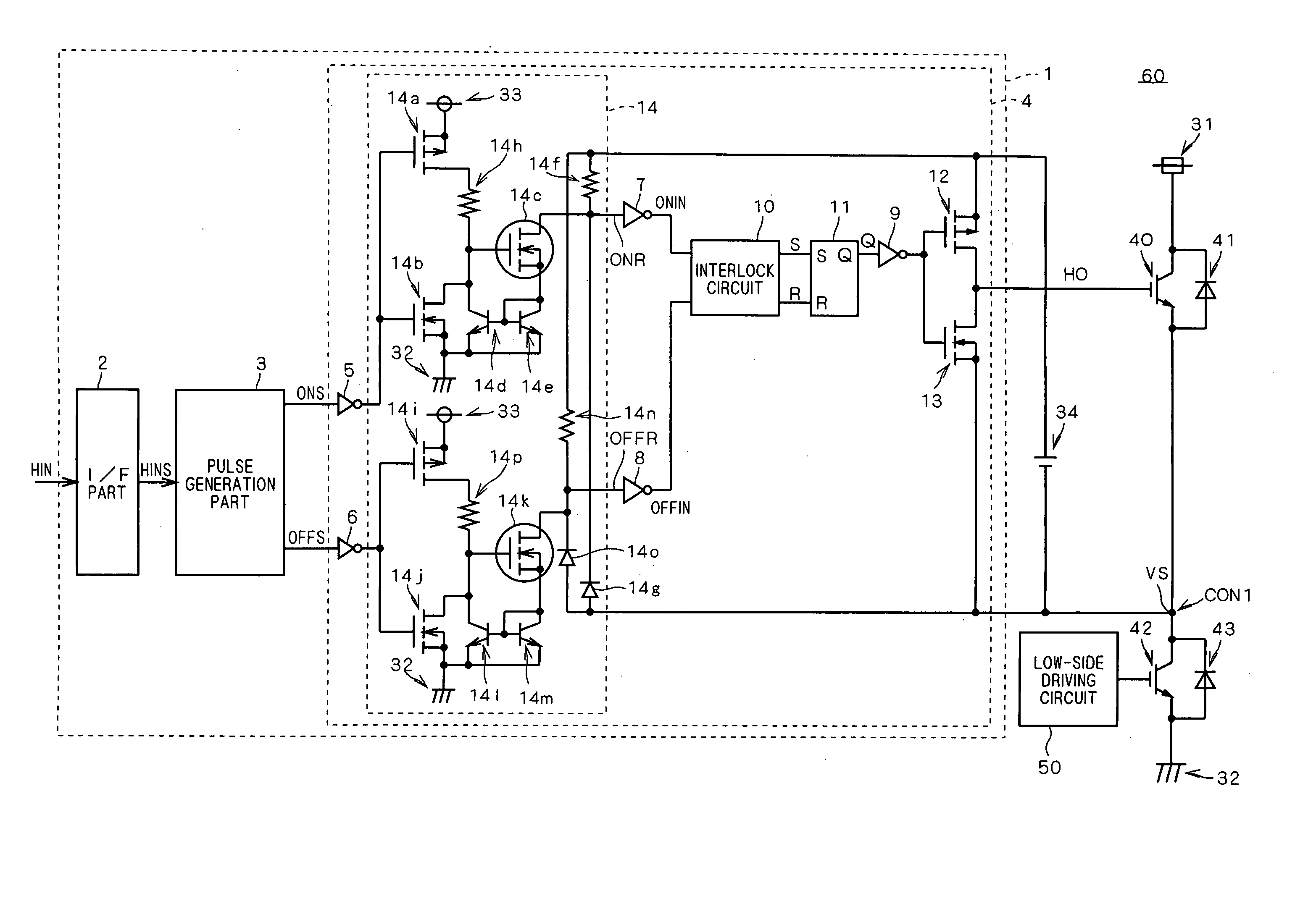
[0027]FIG. 1 is a block diagram showing the configuration of a semiconductor device 60 according to preferred embodiments of this invention. As shown in FIG. 1, the semiconductor device 60 according to the preferred embodiments includes switching devices 40 and 42 both of which are IGBTs, for example, freewheel diodes 41 and 43, a driving circuit 1 for the switching device 40, a driving circuit 50 for the switching device 42, and a power source 34.
[0028] The switching device 40 has a collector connected to a high power supply potential 31 and the cathode of the freewheel diode 41, and an emitter connected to the anode of the freewheel diode 41. The switching device 42 has an emitter connected to a low power supply potential 32 and the anode of the freewheel diode 43, and a collector connected to the cathode of the freewheel diode 43. The emitter of the switching device 40 and the collector of the switching device 42 are connected to each other at a node CON1. A load not shown such ...
second preferred embodiment
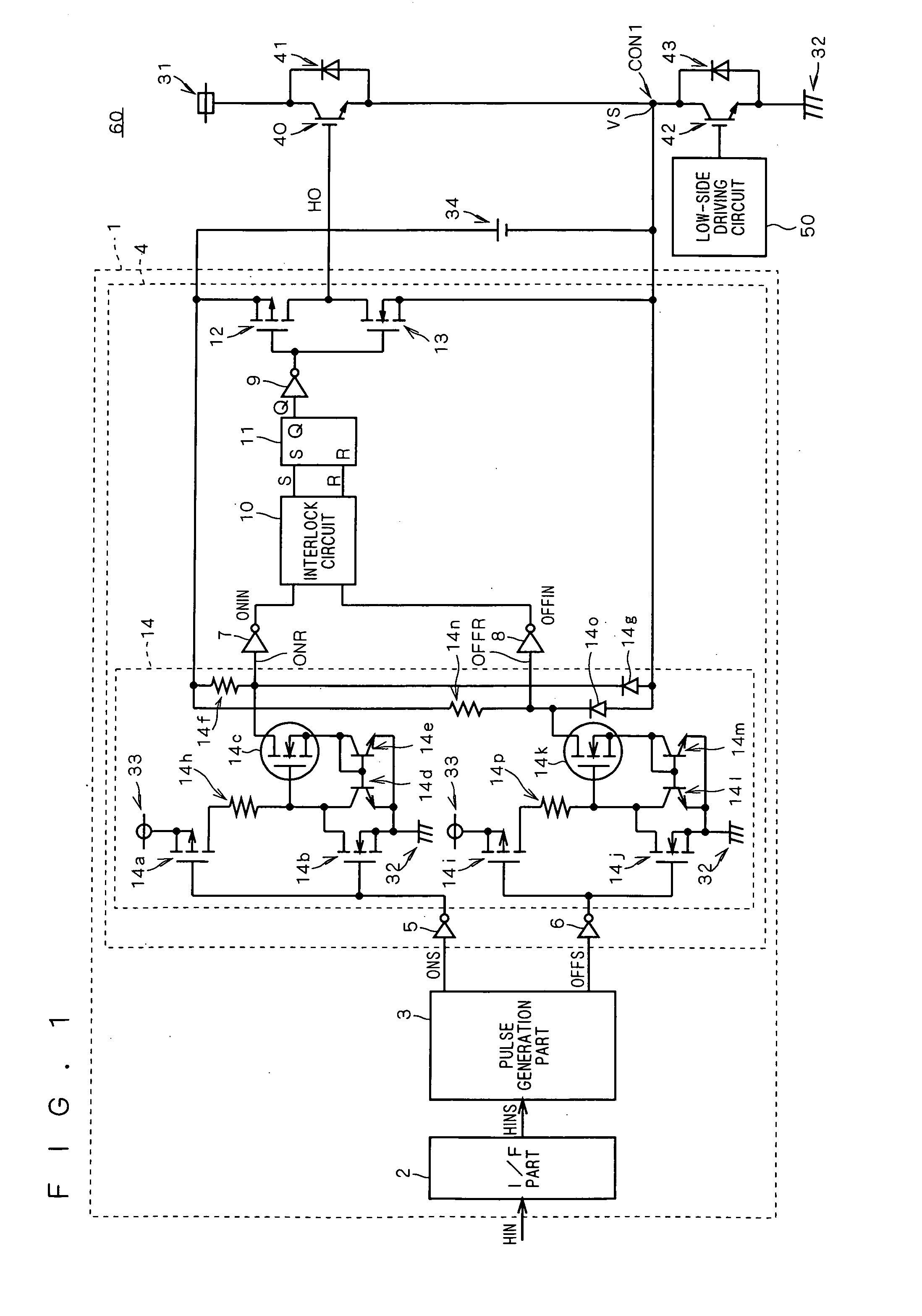
[0098]FIG. 10 is a block diagram showing the configuration of the pulse generation part 3 (see FIG. 1) constituting the semiconductor device 60 according to a second preferred embodiment of the invention. The other elements constituting the semiconductor device 60 are the same as those in the first preferred embodiment and denoted by the same reference numerals, to omit a redundant description.
[0099] As shown in FIG. 10, the pulse generation part 3 includes one-shot pulse generation circuits 4a to 4c, inverters 4d and 4e, a delay circuit 4f, and an NOR circuit 4g. The one-shot pulse generation circuit 4a is adjusted to output a one-shot pulse having a pulse length pw2 greater than the period twd1 based on the trailing edge of the input signal, as shown in FIG. 11. This pulse length pw2 is set by properly adjusting the capacitance of the capacitor 30h (see FIG. 4) in the one-shot pulse generation circuit 4a.
[0100] The signal HINS input from the I / F part 2 is input into the one-shot...
third preferred embodiment
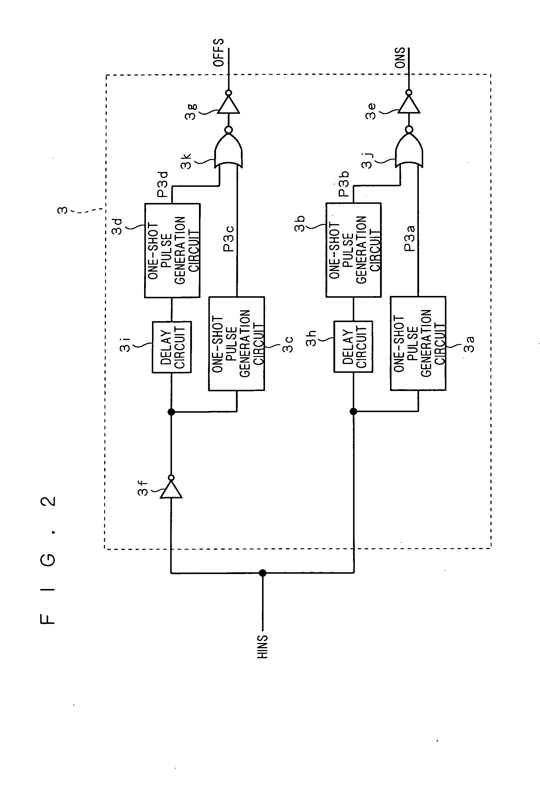
[0109]FIG. 13 is a block diagram showing the configuration of the pulse generation part 3 (see FIG. 1) constituting the semiconductor device 60 according to a third preferred embodiment of the invention. The other elements constituting the semiconductor device 60 are the same as those in the first preferred embodiment and denoted by the same reference numerals, to omit a redundant description. As shown in FIG. 13, the pulse generation part 3 includes one-shot pulse generation circuits 5a to 5e, inverters 5f to 5h, delay circuits 5i to 5k, and NOR circuits 5l and 5m. The configurations and operations of these one-shot pulse generation circuits and delay circuits are the same as those in the first preferred embodiment and explanations thereof are thus omitted.
[0110] The signal HINS input from the I / F part 2 branches into two signals. One signal HINS is input into the inverter 5f which inverts and outputs the signal HINS. The one-shot pulse generation circuit 5d outputs a signal P5d b...
PUM
 Abstract
Description
Claims
Application Information
 - R&D
- Intellectual Property
- Life Sciences
- Materials
- Tech Scout
- Unparalleled Data Quality
- Higher Quality Content
- 60% Fewer Hallucinations
Browse by: Latest US Patents, China's latest patents, Technical Efficacy Thesaurus, Application Domain, Technology Topic, Popular Technical Reports.
© 2025 PatSnap. All rights reserved.Legal|Privacy policy|Modern Slavery Act Transparency Statement|Sitemap|About US| Contact US: help@patsnap.com