Electron emitter and method of producing the same
a technology of electron emitter and emitter, which is applied in the manufacture of electrode systems, discharge tube luminescnet screens, instruments, etc., can solve the problems of high production cost, inability to perform electron emission stably, and inconvenient practical use of conventional electron emitters, and achieve high electron emission efficiency.
- Summary
- Abstract
- Description
- Claims
- Application Information
AI Technical Summary
Benefits of technology
Problems solved by technology
Method used
Image


Examples
first embodiment
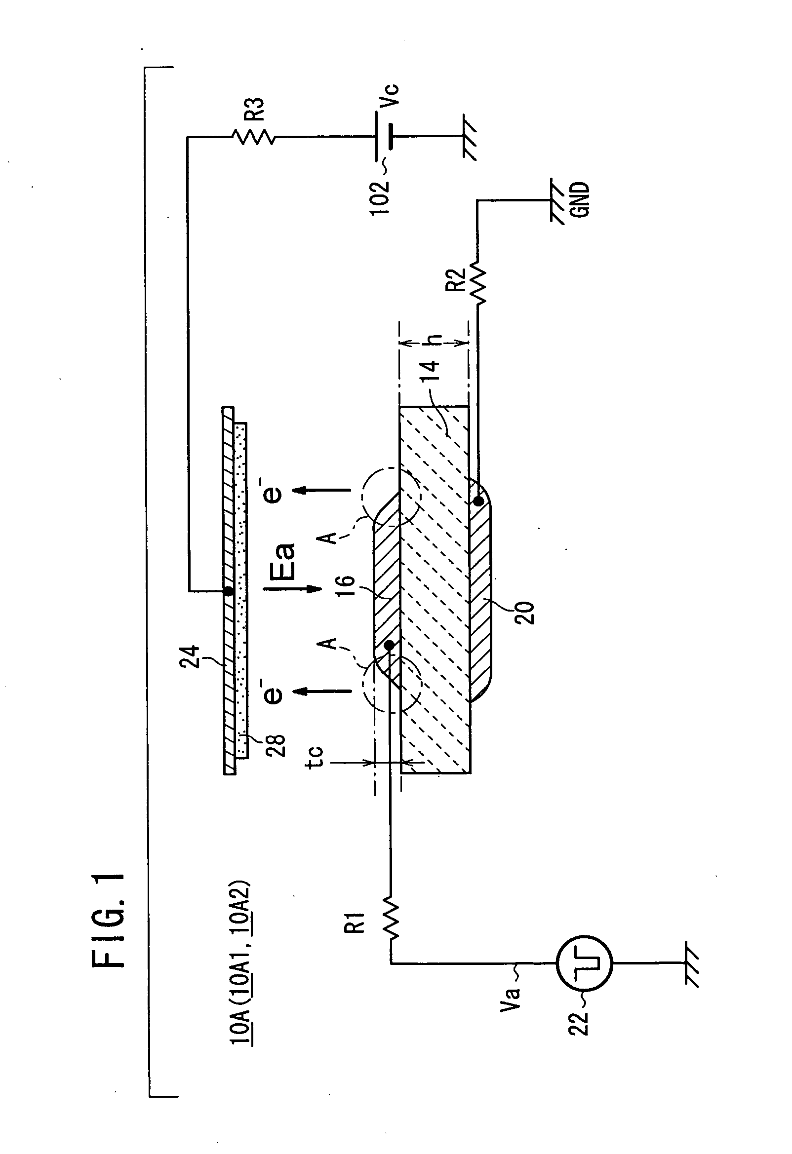
[0112] As shown in FIG. 1, an electron emitter 10A has an emitter section (substance serving as an emitter) 14 having a plate shape, a first electrode (cathode electrode) 16 formed on a front surface of the emitter section 14, a second electrode (anode electrode) 20 formed on a back surface of the emitter section 14, and a pulse generation source 22. A drive voltage Va from a pulse generation source 22 is applied between the cathode electrode 16 and the anode electrode 20 through a resistor R1.
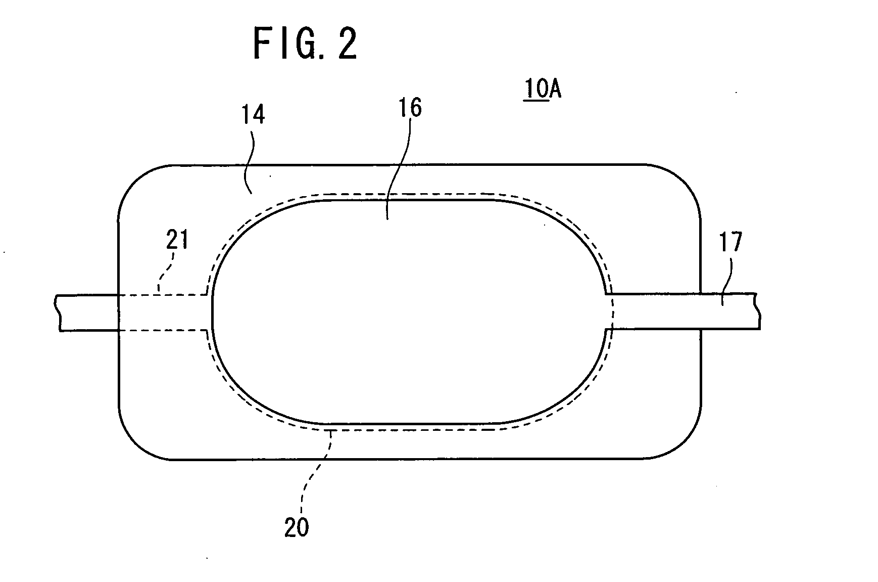
[0113] In an example shown in FIG. 1, the anode electrode 20 is connected to GND (ground) through a resistor R2 and hence set to a zero potential. However, the anode electrode 20 may be set to a potential other than the zero potential. As shown in FIG. 2, the drive voltage Va is applied between the cathode electrode 16 and the anode electrode 20 through a lead electrode 17 extending from the cathode electrode 16 and a lead electrode 21 extending from the anode electrode 20, for example.
[0114...
second embodiment
[0224] Next, an electron emitter 10B will be described.
[0225] The structure of the electron emitter 10B according to the second embodiment is substantially similar to the structure of the electron emitter 10A according to the first embodiment, however, differs in that a plurality of electron emitters 10(1), 10(2), 10(3) are formed on one substrate 12 as shown in FIG. 25.
[0226] That is, in the electron emitter 10B, anode electrodes 20a, 20b, 20c are independently formed on a surface of one substrate 12. Emitter sections 14a, 14b, 14c are formed on upper surfaces of the anode electrodes 20a, 20b, 20c, respectively. Further, cathode electrodes 16a, 16b, 16c are formed on the emitter sections 14a, 14b, 14c, respectively. The emitter sections 14a, 14b, 14c are interposed between the anode electrodes 20a, 20b, 20c, and the cathode electrodes 16a, 16b, 16c, respectively. Slits 80 are formed between the electron emitter 10(1) and the electron emitter 10(2), and between the electron emitte...
third embodiment
[0257] Next, an electron emitter 10C will be described with reference to FIG. 30.
[0258] As shown in FIG. 30, the structure of the electron emitter 10C according to the third embodiment 10C is substantially similar to the structure of the electron emitter 10A according to the first embodiment, however, differs in that the electron emitter 10C has one substrate 110 made of, e.g., ceramics, the anode electrode 20 is formed on the surface of the substrate 110, the emitter section 14 is formed on the substrate 110 to cover the anode electrode 20, and the cathode electrode 16 is formed on the emitter section 14.
[0259] A space 112 is formed in the substrate 110 at a position for forming each emitter section 14. The space 112 forms a thin wall section as described later. The space 112 is connected to the outside through a small diameter through hole 114 provided on the other surface of the substrate 110.
[0260] The substrate 110 has a thin region where the space 112 is formed. The thin re...
PUM
 Abstract
Description
Claims
Application Information
 - R&D
- Intellectual Property
- Life Sciences
- Materials
- Tech Scout
- Unparalleled Data Quality
- Higher Quality Content
- 60% Fewer Hallucinations
Browse by: Latest US Patents, China's latest patents, Technical Efficacy Thesaurus, Application Domain, Technology Topic, Popular Technical Reports.
© 2025 PatSnap. All rights reserved.Legal|Privacy policy|Modern Slavery Act Transparency Statement|Sitemap|About US| Contact US: help@patsnap.com