Solid-state radiation imager with back-side irradiation

a radiation imager and solid-state technology, applied in the field of solid-state radiation imagers, can solve the problems of image blurring, difficult distance, and the likelihood of spreading away

Active Publication Date: 2005-04-07
GENERAL ELECTRIC CO
View PDF9 Cites 42 Cited by
  • Summary
  • Abstract
  • Description
  • Claims
  • Application Information

AI Technical Summary

Problems solved by technology

A problem that arises as the thickness of the scintillator increases is that blurring of the image occurs.
The distance is problematic because not all light photons will propagate to the pixelated array of photosensitive elements since the light emanates isotropically in all directions.
The more distance that light has to travel to reach the pixelated array of photosensitive elements increases the likelihood of it spreading away from the array, which affects the energy level detected by the array and results in blurring.
Although the scintillator needles are helpful in directing the light photons towards the pixelated array of photosensitive elements, some spreading of the light still does occur, which results in blurring.

Method used


Image

  • Solid-state radiation imager with back-side irradiation
  • Solid-state radiation imager with back-side irradiation
  • Solid-state radiation imager with back-side irradiation

Examples


Embodiment Construction

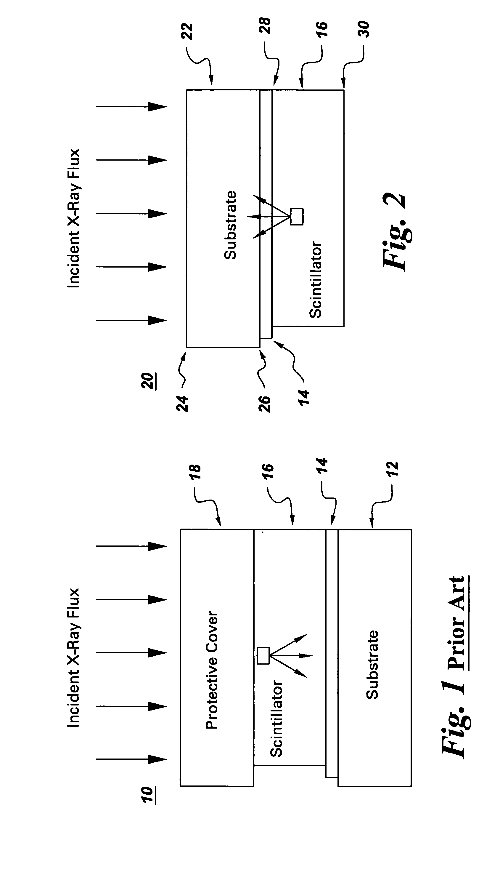
[0020]FIG. 1 is a schematic of a cross-sectional view of a solid-state radiation imager 10 such as an x-ray imager according to the prior art. The imager 10 comprises an x-ray opaque substrate 12. In large flat panel imagers (e.g., imagers greater than 10 cm×10 cm), the substrate 12 is typically comprised of glass. An example of an x-ray opaque substrate is a CORNING 1.1 mm 1737 substrate that has been doped with elements having a high atomic number (Z) such as Barium to provide special properties that can withstand stringent manufacturing specification required for semiconductor processing. This type of substrate has a very poor x-ray transmission. For example, the CORNING 1.1 mm 1737 substrate has an x-ray transmission that is less than 15% for a typical radiation spectrum used for mammography x-ray applications and less than 70% for a typical spectrum used for vascular x-ray applications.

[0021] The x-ray imager 10 also comprises a pixelated array of photosensitive elements 14 di...


PUM


Abstract

A solid-state imager with back-side irradiation. The present invention provides a solid-state imager that includes a substantially radiation transparent substrate adapted to receive incident radiation. The radiation travels through the substrate and a pixelated array of photosensitive elements to a scintillator material, which absorbs the radiation. The pixelated array of photosensitive elements receives light photons and measures the amount of light generated by radiation interactions with the scintillator material. With this imager, there is less spreading and blurring and thus a better quality image. In another embodiment, there is a substantially transparent material disposed between the pixelated array of photosensitive elements and the scintillator material. The substantially transparent material absorbs and substantially blocks electrons from entering the active regions of the pixelated array of photosensitive elements. This enables the imager to perform for a longer period of time according to its specifications.

Description

BACKGROUND OF THE INVENTION [0001] This invention relates generally to solid-state radiation imagers and more particularly to improving the spatial resolution of solid-state radiation imagers through back-side irradiation. [0002] A typical solid-state radiation imager such as an x-ray imager uses a pixelated array of photosensitive elements fabricated on a substrate that is at least partially x-ray opaque. A scintillator coupled to the pixelated array of photosensitive elements receives incident x-rays. Some x-ray imagers have an x-ray transparent protective cover disposed over the scintillator to provide protection for the scintillator. In typical operation, incident x-rays pass through the protective cover into the scintillator. The scintillator absorbs the x-rays and generates light photons that emanate isotropically in all directions. The pixelated array of photosensitive elements receives the light photons that propagate through the scintillator. The pixelated array of photosen...

Claims


Application Information

Patent Timeline
Patent Type & Authority Applications(United States)
IPC IPC(8): G01T1/20G01T1/24H01L27/14H01L27/146H01L31/09H01L31/115H04N5/32
CPCG01T1/2018G01T1/2019G01T1/20187
Inventor ALBAGLI, DOUGLASSHIANG, JOSEPH JOHNPOSSIN, GEORGE EDWARDHENNESSY, WILLIAM ANDREW
Owner GENERAL ELECTRIC CO
Why Eureka
Try Eureka