Radiation detector
a detector and radiofrequency technology, applied in the field of radiofrequency detectors, can solve the problems of low-quality radiographic images, defects that cannot be long-term reliable, and could occur, and achieve the effect of improving the bonding property of the common electrod
- Summary
- Abstract
- Description
- Claims
- Application Information
AI Technical Summary
Benefits of technology
Problems solved by technology
Method used
Image
Examples
first embodiment
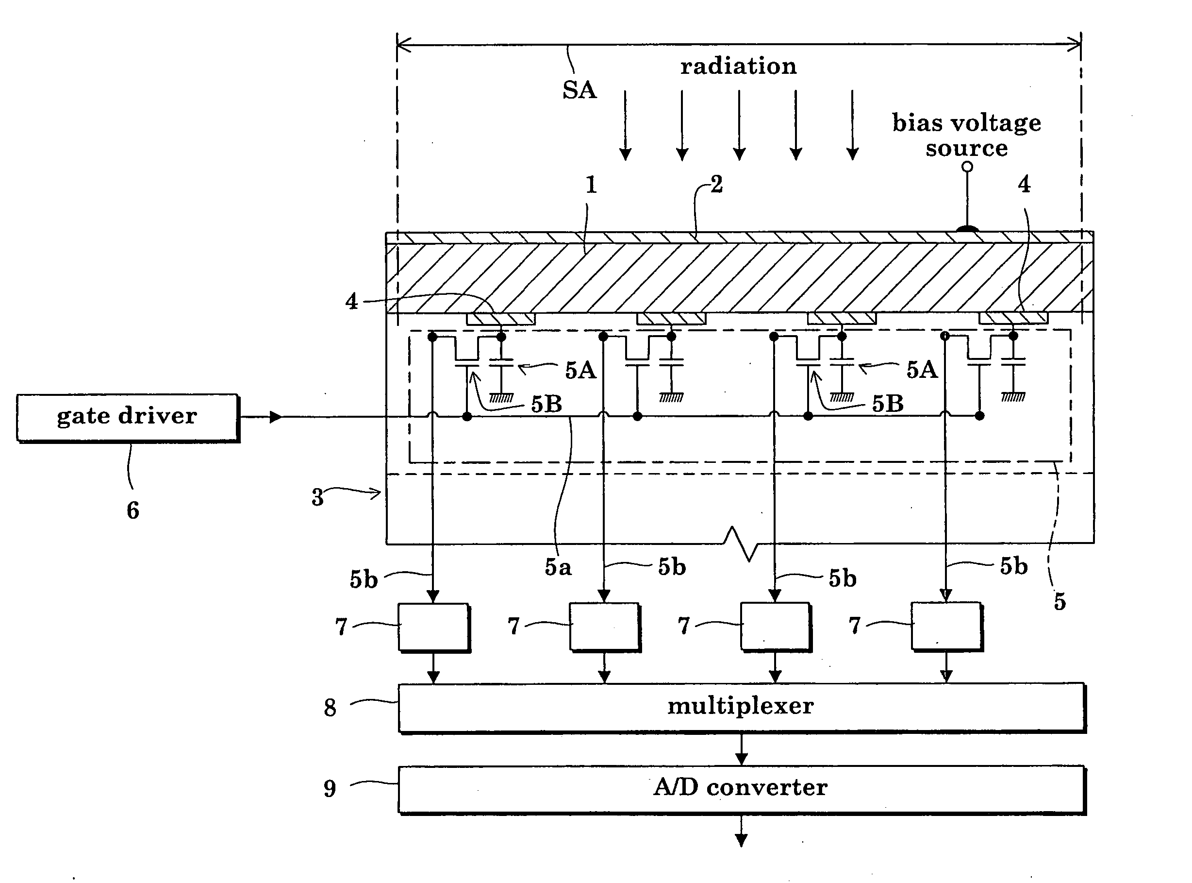
[0045] A radiation detector embodying this invention will be described with reference to the drawings. FIG. 2 is a block diagram showing, in section, a principal portion of a radiation detector of the direct conversion type in a first embodiment of the invention. FIG. 3 is a block diagram showing electric circuits on and around an active matrix substrate of the detector in the first embodiment.
[0046] As shown in FIG. 2, the radiation detector in the first embodiment includes an amorphous selenium semiconductor film (a-Se semiconductor film) 1 sensitive to radiation, and a common electrode 2 for bias voltage application. The common electrode 2 for bias voltage application is formed two-dimensionally on the front surface of the a-Se semiconductor film 1. The detector in the first embodiment includes an active matrix substrate 3. As shown in FIG. 3, numerous collecting electrodes 4 are formed on the surface of the active matrix substrate 3 in a two-dimensional matrix arrangement set w...
second embodiment
[0062] A radiation detector in a second embodiment will be described with reference to the drawings. FIG. 4 is a block diagram showing, in section, a principal portion of a radiation detector of the direct conversion type in the second embodiment of the invention.
[0063] As shown in FIG. 4, the radiation detector in the second embodiment includes a carrier selective intermediate layer 10 formed between the a-Se semiconductor film 1 and common electrode 2, and a carrier selective intermediate layer 11 formed between the a-Se semiconductor film 1 and collecting electrodes 4. The other aspects are the same as in the detector in the first embodiment. Only different features will be described below, and the common features will not be described again.
[0064] The detector in the second embodiment, with the carrier selective intermediate layers 10 and 11, can reduce dark current. The detector in the second embodiment has the common electrode 2 formed on the carrier selective intermediate l...
PUM
 Abstract
Description
Claims
Application Information
 - R&D
- Intellectual Property
- Life Sciences
- Materials
- Tech Scout
- Unparalleled Data Quality
- Higher Quality Content
- 60% Fewer Hallucinations
Browse by: Latest US Patents, China's latest patents, Technical Efficacy Thesaurus, Application Domain, Technology Topic, Popular Technical Reports.
© 2025 PatSnap. All rights reserved.Legal|Privacy policy|Modern Slavery Act Transparency Statement|Sitemap|About US| Contact US: help@patsnap.com


