
Optical receiver circuit

a receiver circuit and optical receiver technology, applied in the direction of transmission, electromagnetic transmission, transmission monitoring, etc., can solve the problems of considerable interference, high cost of considerable additional costs in the production of previously known receiver circuits, so as to achieve high gain, high cost-effectiveness, and high gain

Active Publication Date: 2005-03-03
AVAGO TECH INT SALES PTE LTD
View PDF14 Cites 18 Cited by
  • Summary
  • Abstract
  • Description
  • Claims
  • Application Information

AI Technical Summary

Benefits of technology

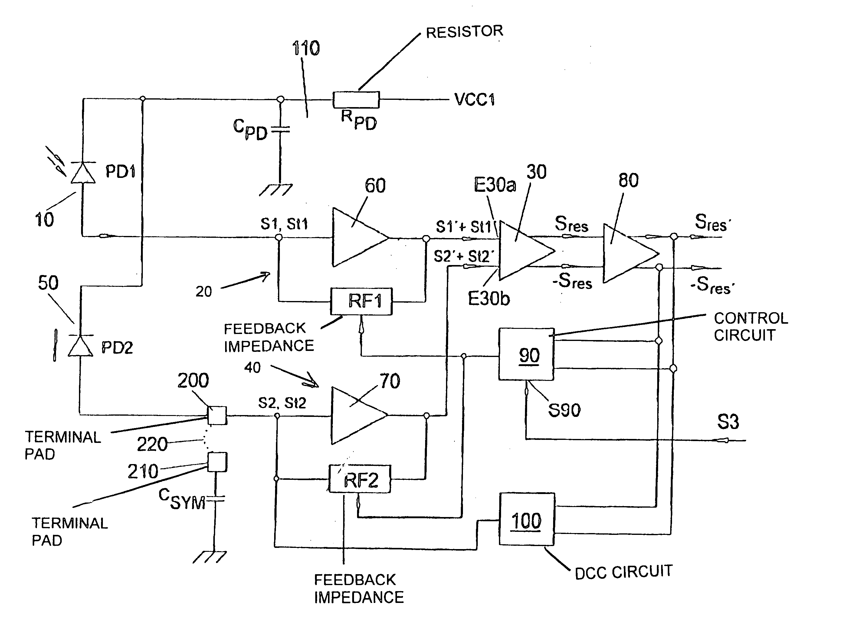
One essential advantage of the optical receiver circuit according to the invention is to be seen in the fact that this receiver circuit is particularly immune to interference. In the receiver circuit according to the invention, this is achieved by means of the “fully differential” design of the circuit or the quasi-symmetrical input-end circuitry of the differential amplifier. In this case, the fully differential design is based on the electrical element according to the invention, which simulates the electrical behavior of the reception device in the illumination-free case. On account of the electrical element, the differential amplifier is connected up symmetrically, so that high-frequency interference is effectively suppressed. This is because high-frequency interference will occur simultaneously on account of the symmetrical input-end circuitry of the differential amplifier at the two inputs of the differential amplifier, so that the interference is suppressed to the greatest possible extent by virtue of the common-mode rejection that is always high in the case of differential amplifiers.
For symmetrical operation of the optical receiver circuit and thus for maximum interference suppression, it is advantageous if the reception device and the simulating electrical element are in each case connected to the same supply voltage. A low-pass filter is preferably connected to the supply voltage, which filter filters out high-frequency interference from the supply voltage.

Problems solved by technology

For this reason, the susceptibility to interference is also very high; this means that high-frequency interference—for example on the supply voltage of the optical receiver circuit and / or received radiated electromagnetic interference (EMI: electromagnetic interference)—can considerably impair the functionality of the optical receiver circuit.
It is evident that these shielding measures lead to considerable additional costs in the production of the previously known receiver circuits.

Method used


Image

  • Optical receiver circuit
  • Optical receiver circuit

Examples


Embodiment Construction

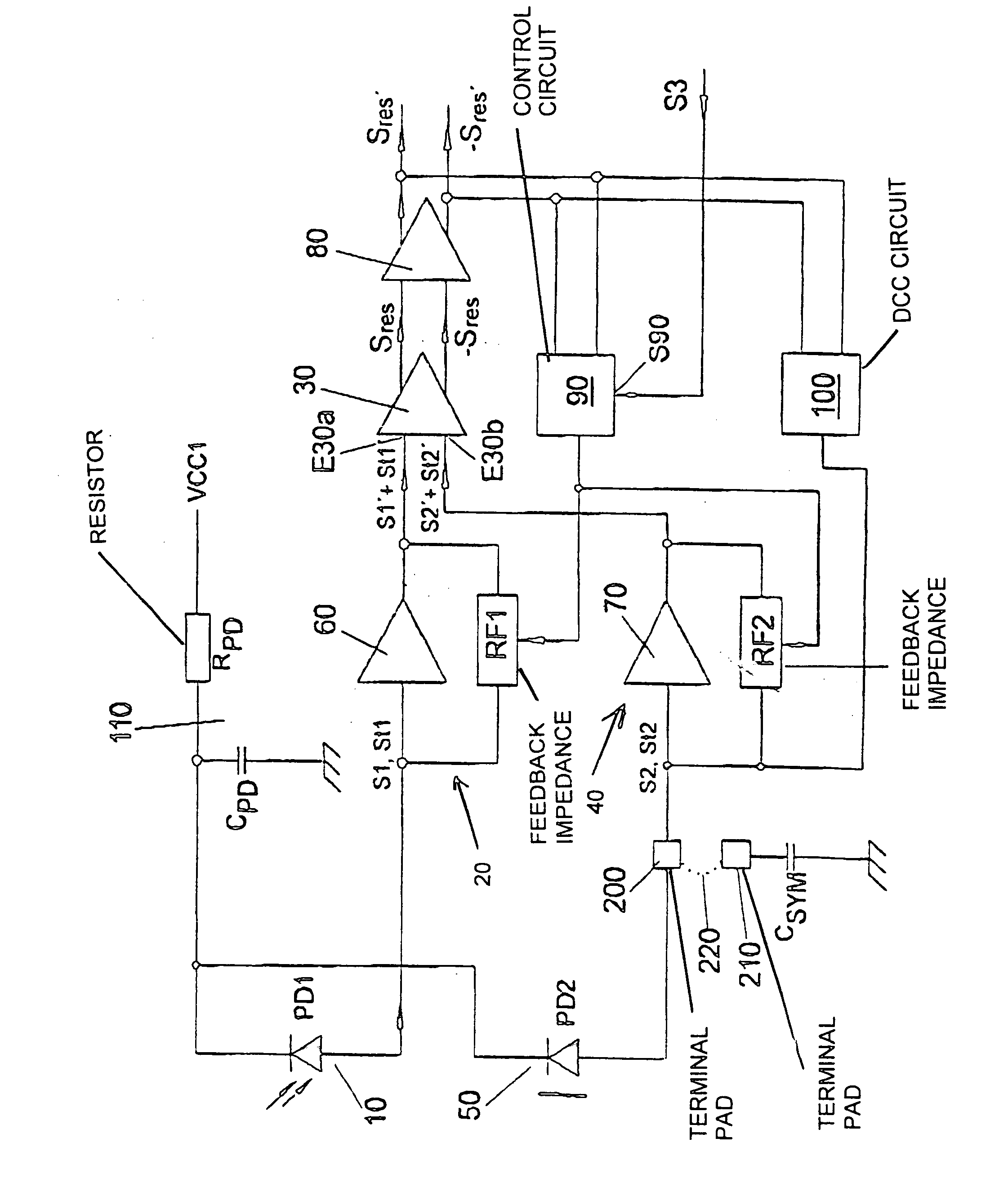
In order to elucidate the invention, a figure shows an exemplary embodiment of an optical receiver circuit according to the invention.

The figure reveals a photodiode 10 as reception device (“useful” reception device), which is connected to one terminal E30a of a differential amplifier 30 via a transimpedance amplifier 20. The other input E30b of the differential amplifier 30 is connected via a further preamplifier 40, embodied as a transimpedance amplifier, to a “dummy” photodiode 50 as “dummy” reception device which electrically simulates the electrical behavior of the reception device 10 in the illumination-free case.

The transimpedance amplifier 20 is formed by a voltage amplifier 60, for example an operational amplifier, which is connected up to a feedback impedance RF1. In a corresponding manner, the further transimpedance amplifier 40 is formed by a voltage amplifier, for example an operational amplifier 70 identical to the operational amplifier 60, which is connected up t...


PUM


Abstract

An optical receiver circuit is constructed to be immune to interference from external interference signals. The optical receiver circuit includes a differential amplifier having an optical reception device connected to one input of the differential amplifier. The optical receiver circuit also includes an electrical element for simulating the electrical behavior of the reception device in the illumination-free state. The electrical element is connected to the other input of the differential amplifier.

Description

TECHNICAL FIELD The invention relates to an optical receiver circuit having an optical reception device and an amplifier device connected downstream. Light incident on the reception device (e.g. photodiode)—for example light from an optical waveguide of an optical data transmission system—is detected by the reception device with formation of an electrical signal (e.g. photocurrent); the electrical signal is subsequently amplified by the amplifier device connected downstream. Optical receiver circuits of this type require a very high sensitivity since the optical light signals to be received and thus the electrical signals formed by the reception device are generally very small. For this reason, the susceptibility to interference is also very high; this means that high-frequency interference—for example on the supply voltage of the optical receiver circuit and / or received radiated electromagnetic interference (EMI: electromagnetic interference)—can considerably impair the functiona...

Claims


Application Information

Patent Timeline
Patent Type & Authority Applications(United States)
IPC IPC(8): H04B10/06H04B10/158
CPCH04B10/6933
Inventor SCHRODINGER, KARL
Owner AVAGO TECH INT SALES PTE LTD
Learn More