Method of improving surface planarity

Active Publication Date: 2005-02-17
UNITED MICROELECTRONICS CORP
View PDF3 Cites 0 Cited by
  • Summary
  • Abstract
  • Description
  • Claims
  • Application Information

AI Technical Summary

Benefits of technology

[0008] Thus, the main object of the present invention is to provide a method of improving surface planarity of a wafer when depositing a plurality of thin-film layers on the wafer using CVD, thereby providing excellent improvement of the surface planarity of the wafer, improving the pattern CD control when defining patterns on every thin-film layer, and enhancing process yield and product reliability.

Problems solved by technology

The uneven surface of thin-film layer 120 may not be successfully focused during pattern definition on the thin-film layer 120, deteriorating the critical dimension (CD) control of the patterns, and thereby negatively affecting yield and reliability.

Method used


Image

  • Method of improving surface planarity
  • Method of improving surface planarity
  • Method of improving surface planarity

Examples


Embodiment Construction

[0015] The following embodiment is intended to illustrate the invention more fully without limiting its scope, since numerous modifications and variations will be apparent to those skilled in this art.

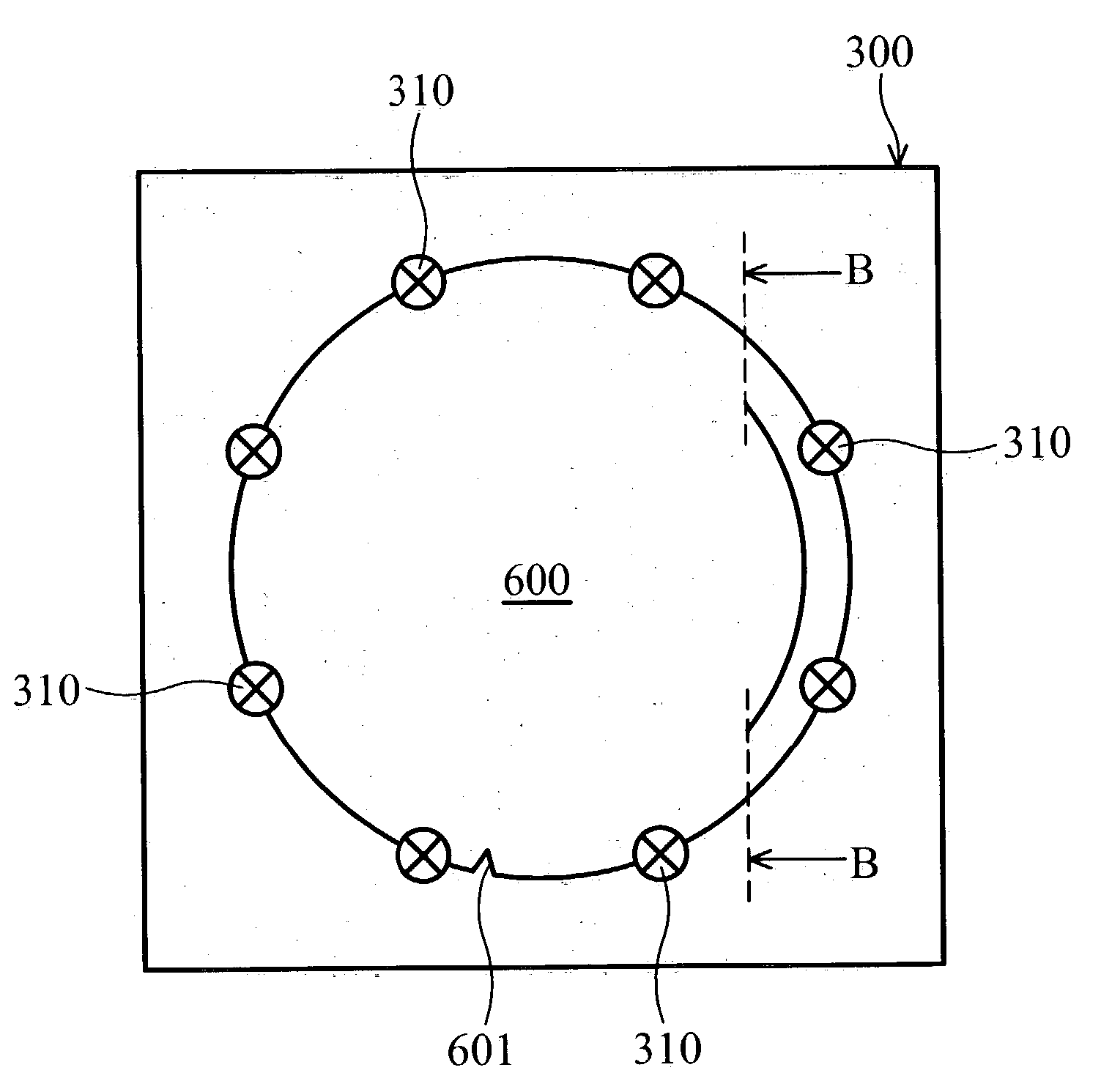
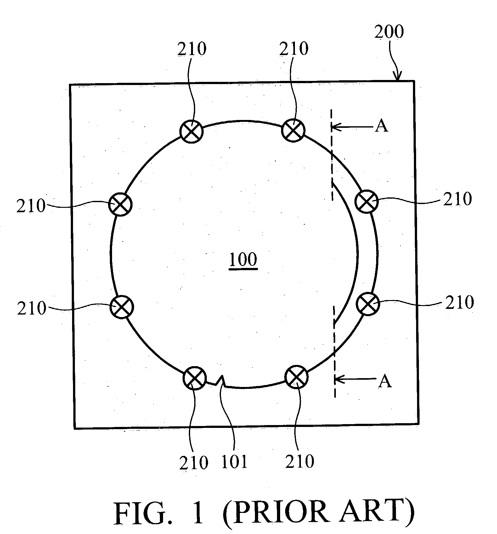
[0016]FIG. 3A is a simplified top view of a wafer 600 in a chamber 300 of a first CVD thin film deposition apparatus (not shown). The chamber 300 has eight gas injectors 310 uniformly arranged in a circle above the wafer 600. When starting CVD, a reactive gas enters the chamber 300 from gas injectors 310 and starts a chemical reaction to deposit a thin-film layer such as dielectric on the wafer 600. The wafer 600 has an alignment element such as a notch 601 to enable orientation thereof.

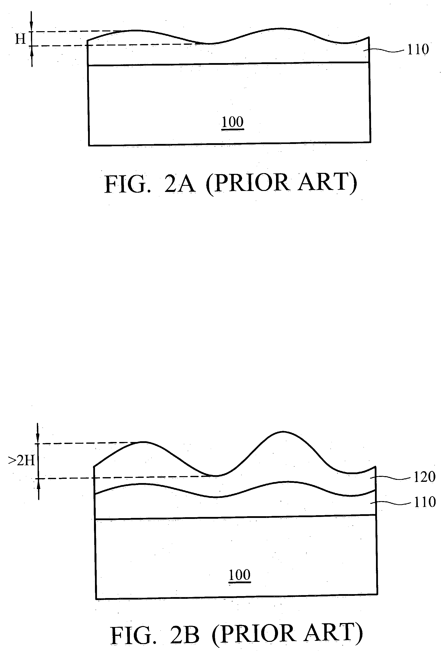
[0017]FIG. 4A is a cross-section of the profile of wafer 600 along arc BB in FIG. 3A after thin film deposition and planarization in which thin-film layer 610, such as a dielectric layer, is formed by CVD. The concentration of the reactive gas is higher near the gas injectors 310, such that proximity ...


PUM

PropertyMeasurementUnit
Timeaaaaaaaaaa
Angleaaaaaaaaaa
Dielectric polarization enthalpyaaaaaaaaaa

Abstract

A method of improving surface planarity of a wafer. The method includes forming a first thin-film layer on the wafer using CVD in a first thin film deposition apparatus having at least one gas injector, relative to which the wafer has a first orientation, and forming a second thin-film layer on the wafer using CVD. The second deposition takes place in a second thin film deposition apparatus having at least one second gas injector arranged the same as that in the first thin film deposition apparatus, the wafer having a second orientation relative to the gas injector in the second thin film deposition apparatus. A first angle between the two orientations results in the second apparatus' injector distributing material in a different area from that of the first gas injector.

Description

BACKGROUND OF THE INVENTION [0001] 1. Field of the Invention [0002] The present invention relates to a method of fabricating a semiconductor device, and more specifically to a method of improving surface planarity of a wafer when depositing a plurality of thin-film layers using chemical vapor deposition (CVD). [0003] 2. Description of the Related Art [0004]FIG. 1 is a simplified top view of a wafer 100 in a chamber 200 of a CVD thin film deposition apparatus (not shown). The chamber 200 has eight gas injectors 210 uniformly arranged in a circle above the wafer 100. When starting CVD, a reactive gas enters the chamber 200 from gas injectors 210 and starts a chemical reaction to deposit a thin-film layer such as dielectric on the wafer 100. [0005]FIG. 2A is a cross-section of the profile of wafer 100 along arc AA in FIG. 1 after thin film deposition and planarization. A thin-film layer 110, such as a dielectric layer, is formed by CVD on the wafer 100. The concentration of the reactiv...

Claims


Application Information

Patent Timeline
IPC IPC(8): C23C16/455H01L21/316
CPCH01L21/31604C23C16/455H01L21/02271H01L21/022
Inventor CHAN, CHIEN-CHINGOUYANG, YUN-LIANGLU, YUNG-WEI
Owner UNITED MICROELECTRONICS CORP
Why Eureka
Try Eureka