Amplifier circuit with active gain step circuit

Active Publication Date: 2005-02-03
INFINEON TECH AG
View PDF7 Cites 3 Cited by
  • Summary
  • Abstract
  • Description
  • Claims
  • Application Information

AI Technical Summary

Benefits of technology

[0010] It is the object of the present invention to provide an amplifier circuit with a main stage amplifier and a secondary stage amplifier where a load of the RF input is reduced.
[0015] The bias voltages of the input bipolar transistor and the output bipolar transistor in the switched-on state of the secondary stage amplifier can be provided by a common bias supply or by separate bias supplies for the input bipolar transistor and the output bipolar transistor, which enables a higher flexibility.
[0016] The terminal of the input bipolar transistor and the output bipolar transistor, which is not coupled to the RF input and the RF output, respectively, i.e. normally their emitter terminal, is connected to a reference potential, normally mass, via a respective resistor. Thus, the input impedance and the output impedance of the gain step circuit can easily be set by modifying the transistor size and the named resistors, so that these impedances have the same or similar values like the main stage. This property enables a good matching at the input / output in the secondary stage. Additionally, the matching of the main stage is only insignificantly changed.
[0017] By the inventive design, the gain step circuit, i.e. the secondary stage amplifier, consumes a lower operating current than the main stage amplifier. Above that, the forward transmission factor in the secondary stage can easily be set by resistors and the control current, which is supplied by the supply voltage, and can easily be varied in a wider range in comparison to passive gain step circuits for different applications. Thus, in the secondary stage, higher IP3 values (IP3=third order intercept point) can be obtained with lesser current consumption.
[0018] If the secondary stage is switched-off, the collector base diode of the input bipolar transistor and the collector base diode of the output bipolar transistor are reverse-biased. Thus, a good isolation of the gain step circuit to the main stage amplifier is enabled by the low barrier layer capacity of these diodes. This makes possible the already mentioned separation of the design of the circuit for the main stage and for the secondary stage, which leads to decreased development times.
[0019] The principle underlying the present invention consists of the combination of the input via the input bipolar transistor, and the output via the output bipolar transistor, wherein (in preferred embodiments) collector base diode paths, or (in less preferred embodiments) emitter base diode paths, respectively, of the input bipolar transistor and the output bipolar transistor are switched into the RF path. Thereby, a main stage in a common emitter circuit is loaded only minimally and the input matching and the output matching for all stages is made significantly easier.

Problems solved by technology

These secondary stages generate a capacity in parallel to the main stage, and thus reduce the performance of the main stage.
The same problem holds true, in a slightly reduced form, for the output side of the amplifier arrangement, since the secondary stage of several secondary stages are connected in parallel between the RF input and the RF output.
Passive gain step circuits do not provide an amplification between the RF input and the RF output, when they are switched on.
However, a disadvantage of the above described solution is that the main stage is significantly loaded with the capacities of the transistor T1 in a range of 200 to 400 fF at the RF input.
This leads to a significant deterioration of the performance of the main stage amplifier with regard to amplification and noise performance.

Method used


Image

  • Amplifier circuit with active gain step circuit
  • Amplifier circuit with active gain step circuit
  • Amplifier circuit with active gain step circuit

Examples


Embodiment Construction

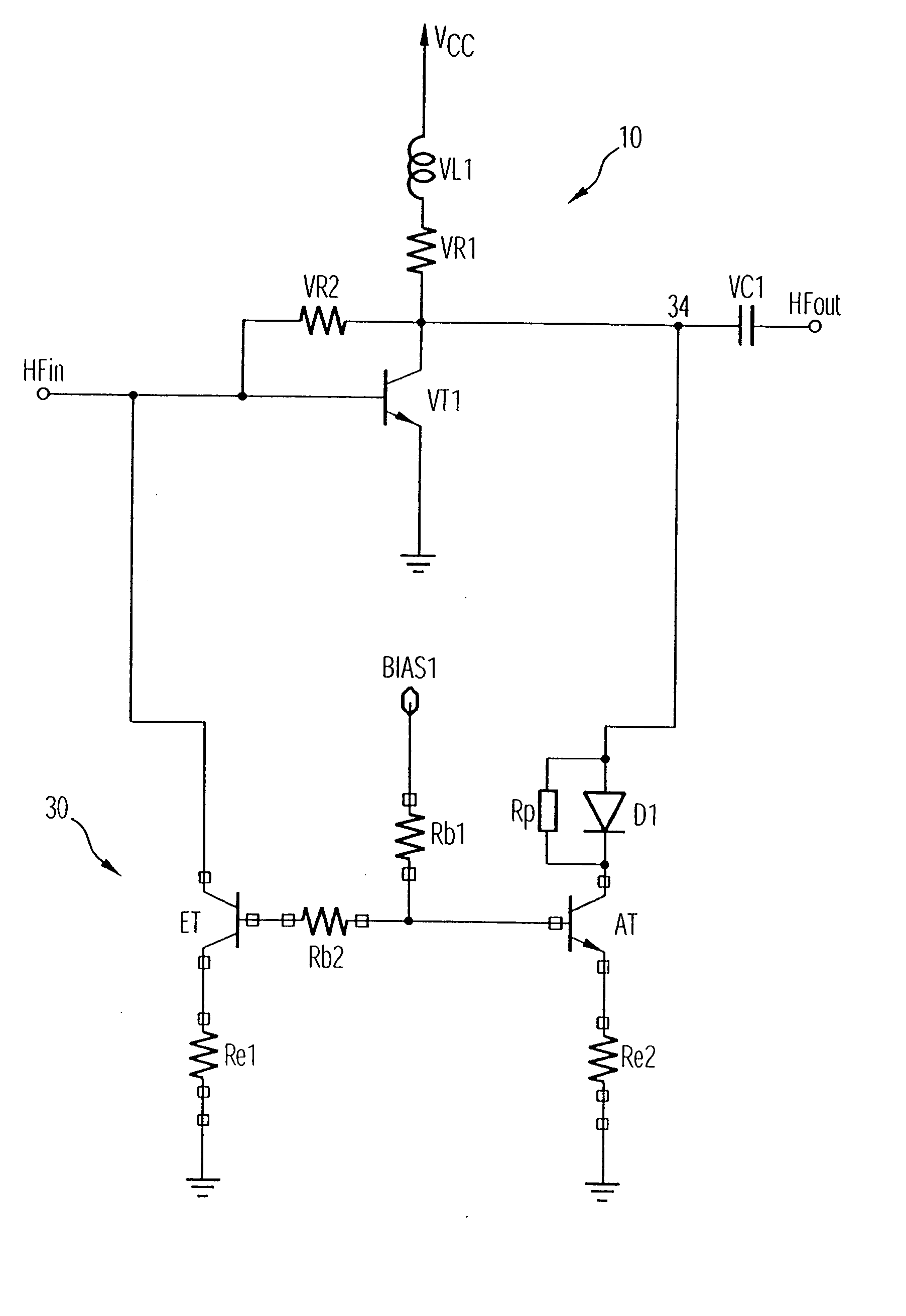
[0026] With reference to FIGS. 3 and 4, a first embodiment of an inventive amplifier circuit will be discussed below in more detail, wherein first a secondary stage amplifier is addressed with reference to FIG. 3.

[0027] The secondary stage amplifier 30 comprises an input bipolar transistor ET and an output bipolar transistor AT. The input terminal of the input bipolar transistor ET is connected to the RF input HFin. The emitter terminal of the input bipolar transistor ET is connected to a reference potential, in the shown embodiment ground, via a resistor Re1. The collector terminal of the output bipolar transistor AT is high frequency-coupled to the RF output RFout, in the illustrated embodiment via a diode D1 and a decoupling capacity C1. Further, the collector terminal of the output bipolar transistor AT is connected to a supply voltage terminal 32 via the diode D1, across which a supply voltage is applied, which operates the diode D1 in flow direction and provides the operating...


PUM


Abstract

An amplifier circuit comprises a main stage amplifier connected between a RF input and a RF output and at least one secondary stage amplifier, which is connected in parallel to the main stage amplifier between the RF input and the RF output. The secondary stage amplifier comprises an input bipolar transistor, whose collector terminal or emitter terminal is high frequency-coupled to the RF input. The secondary stage amplifier further comprises an output bipolar transistor, whose base terminal is high frequency-coupled to the base terminal of the input bipolar transistor and whose collector terminal or emitter terminal is high frequency-coupled to the RF output. The output bipolar transistor is further coupled to a supply voltage terminal.

Description

BACKGROUND OF THE INVENTION [0001] 1. Field of the Invention [0002] The present invention relates to an amplifier circuit, and particularly to an amplifier circuit, which has a main stage amplifier and at least one secondary stage amplifier, so that the amplifier circuit allows to switch between the main stage amplifier and the secondary stage amplifier in dependency on the input signal. [0003] 2. Description of Prior Art [0004] In low-noise high frequency amplifiers with high amplification, which are referred to as LANs (LAN=low noise amplifier), it is very important to provide as little load as possible to the high frequency input. If, however, several amplification stages are required, between which a switch-over can be performed, as it can be particularly the case in the field of mobile telecommunication and there, particularly, with mobile telephones, they also have to be coupled to the RF input. These secondary stages generate a capacity in parallel to the main stage, and thus...

Claims


Application Information

Patent Timeline
IPC IPC(8): H03F3/19H03F3/343H03G1/00
CPCH03F3/19H03F3/3432H03G1/0088H03F2200/372H03F2200/294
Inventor LIN, CHIH-ISCHEIBLHOFER, KLAUS
Owner INFINEON TECH AG
Why Eureka
Try Eureka