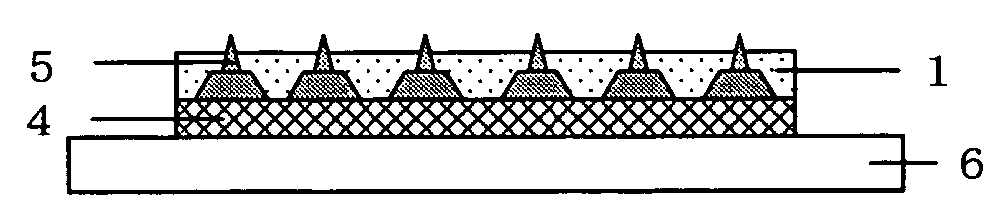
Laminated sheet

a technology of laminated sheets and sheets, applied in the field of laminated sheets, can solve the problems of low mechanical strength of thin wafers subjected to grinding, low reliability of connection, solder balls, etc., and achieve excellent electrical connection reliability, excellent packing property of bumps, and excellent workability of wafers.

Inactive Publication Date: 2005-01-13
NITTO DENKO CORP
View PDF9 Cites 38 Cited by
  • Summary
  • Abstract
  • Description
  • Claims
  • Application Information

AI Technical Summary

Benefits of technology

Accordingly, an object of the present invention is to provide a laminated sheet which can be suitably used in flip-chip mounting, and is excellent in packing property of bumps, gives excellent workability of a wafer, and provides excellent electric connection reliability after resin encapsulation, a method for manufacturing a semiconductor device using the sheet, and a semiconductor device which can be manufactured by the method.

Problems solved by technology

There has been a defect that a thin wafer subjected to grinding has a low mechanical strength against an external force.
However, in order to form electrodes for mounting a semiconductor device on a wiring circuit board, there arises a problem that complicated steps of opening holes corresponding to the positions of the electrodes of the wafer in the resin-encapsulating layer, embedding solders to the open holes, and thereafter forming solder balls in the holes are necessitated.
In this case, since the adhesive film layer completely covers the projection electrodes, the adhesive film layer which is an insulation is mechanically pushed away in an electric connection with the circuit board, so that electric connection must be secured, thereby causing a problem in connection reliability.
Also, since the adhesive film layer completely covers the projection electrodes, a resin is applied in an amount exceeding that required for filling the gap between the semiconductor elements and the circuit board, so that an excess resin is pressed out in a wide range in the surroundings of the semiconductor elements after mounting the chips, thereby causing some problems in high-density mounting.
Since a preferred embodiment proposes to drop a thermoplastic resin which plasticizes at about 150° C., while heating to 240° to 260° C., there arises a problem of failure in transporting the wafer by generation of bowing accompanied by the residual stress of the thermoplastic resin in the wafer after grinding.

Method used


Image

  • Laminated sheet
  • Laminated sheet
  • Laminated sheet

Examples


examples

The present invention will be described more specifically by means of the following Examples, without intending to limit the scope of the present invention thereto.

Raw materials and parts used in Examples are collectively listed hereinbelow.

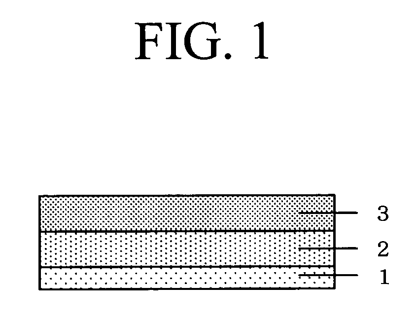
In the formation of the layer A, there were used a naphthalenic epoxy resin (epoxy equivalence: 141 g / eq.) as an epoxy resin, a xylylenic phenolic resin (hydroxyl equivalence: 174 g / eq.) as a curing agent, a microcapsulated triphenylphosphine (TPP) (shell: polyurea, core / shell ratio: 3 / 7 (wt / wt)) as a latent curing accelerator, an acrylonitrile-butadiene copolymer (degree of acrylonitrile bonds: 27%, Moonie viscosity: 70ML1+4 / 100° C.) as a thermoplastic resin, and a spherical silica (average particle size: 2 μm, a maximum particle size: 5 μm) as an inorganic filler.

In the formation of the layer B, an acrylic-urethane composite polymer, a polyvinyl chloride or polyethylene vinyl acetate was used.

In the formation of the layer C, polyethyle...


PUM

PropertyMeasurementUnit
temperatureaaaaaaaaaa
thicknessaaaaaaaaaa
thicknessaaaaaaaaaa

Abstract

A laminated sheet for adhering to a circuit side of a projected electrode-mounting wafer in a step of grinding a backside of the wafer, wherein the laminated sheet comprises at least a layer (layer A) contacting with the circuit side, made of a thermosetting resin, a layer (layer B) directly laminated on the layer A, made of a thermoplastic resin having a tensile modulus of from 1 to 300 MPa at 40° to 80° C., and an outermost layer (layer C) made of a thermoplastic resin which is non-plastic at a temperature of at least 25° C.; A method for manufacturing a semiconductor device, comprising the steps of grinding a backside of a projected electrode-mounting wafer wherein the laminated sheet is adhered to a circuit side of the wafer, removing other layers besides the layer A of the laminated sheet, and cutting the wafer into individual chips; and a semiconductor device obtainable by the method.

Description

BACKGROUND OF THE INVENTION 1. Field of the Invention The present invention relates to a laminated sheet usable in the manufacture of a semiconductor device, a method for manufacturing a semiconductor device using the sheet, and a semiconductor device which can be manufactured by the method. 2. Discussion of the Related Art As the recent requirements accompanied by multi-functionality and miniaturization of a semiconductor device, a flip-chip mounting in which a semiconductor element is mounted on a wiring circuit board with a facedown structure has been carried out. Generally, in the flip-chip mounting, resin encapsulation is carried out at a gap between a semiconductor element and a wiring circuit board in order to protect the semiconductor element. A conventional manufacturing method with flip-chip mounting comprises the step of creating patterns on a wafer, forming bumps, grinding the wafer to a given thickness, cutting the wafer into individual semiconductor elements, and ...

Claims


Application Information

Patent Timeline
Patent Type & Authority Applications(United States)
IPC IPC(8): B32B27/00B32B27/08H01L21/00H01L21/304H01L21/56H01L21/60H01L21/68H01L23/00H01L23/12H01L23/28H01L23/29H01L23/31
CPCB32B27/08H01L21/56H01L21/6835H01L21/6836H01L23/3114H01L23/3157H01L24/27H01L2221/68327H01L2221/6834H01L2221/68363H01L2224/1134H01L2224/131H01L2224/13111H01L2224/13139H01L2224/13144H01L2224/13147H01L2224/274H01L2224/81203H01L2224/81205H01L2224/8121H01L2224/81815H01L2224/83191H01L2924/01005H01L2924/01012H01L2924/01013H01L2924/01015H01L2924/01027H01L2924/01029H01L2924/01033H01L2924/0104H01L2924/01047H01L2924/0105H01L2924/01078H01L2924/01079H01L2924/01082H01L2924/3025H01L24/29H01L2924/00013H01L2924/01006H01L2924/01019H01L2924/014H01L2924/0132H01L2924/0133H01L2924/15787H01L2924/15788H01L2924/1579H01L2224/16225H01L2224/29111H01L2224/32225H01L2224/73104H01L2224/73204H01L2224/2919H01L2924/07802H01L2224/81191Y10T428/24942Y10T428/24802Y10T29/49002Y10T428/265Y10T428/12528H01L2924/00014H01L2224/13099H01L2924/01028H01L2924/3512H01L2924/00Y10T428/31551Y10T428/31565H01L23/12H01L23/28B32B27/26B32B27/38B32B2457/00
Inventor NORO, HIROSHIAKAZAWA, KOJIYAMAMOTO, MASAYUKIYAMAMOTO, YASUHIKO
Owner NITTO DENKO CORP
Why Eureka
Try Eureka