Adapting scan-bist architectures for low power opertation

a scan-bist architecture and low-power technology, applied in the field of adapting scan-bist architectures for low-power opertation, can solve the problems of increasing the cost of manufacturing the ic, prolonging the powerup-self-test time of the ic in portable, battery-operated systems, and adding undesirable delays, so as to achieve less operational power

Inactive Publication Date: 2005-01-06
TEXAS INSTR INC
View PDF4 Cites 4 Cited by
  • Summary
  • Abstract
  • Description
  • Claims
  • Application Information

AI Technical Summary

Benefits of technology

[0015] Scan-BIST architectures are commonly used to test digital circuitry in integrated circuits. The present invention describes a method of adapting conventional Scan-BIST architectures into low power Scan-BIST architectures. The low power Scan-BIST architecture maintains the test time of Scan-BIST architectures, while requiring significantly less operational power than conventional Scan-BIST architectures. The low power Scan-BIST architecture is advantageous to IC / die manufacturers since it allows a larger number of circuits (such as DSP or CPU core circuits) embedded in an IC / die to be tested in parallel without consuming too much power within the IC / die. It is also advantageous to designers of portable, battery operated systems, like wireless telephones, since ICs in the systems can be powerup-self-tested by the low power Scan-BIST architecture using only a fraction of the stored battery energy required by conventional scan-BIST architectures.
[0016] The present invention described below provides a method of adapting synthesized Scan-BIST architectures to achieve a low power mode of operation. The process of adapting Scan-BIST architectures or low power operation is achieved without having to modify the above mentioned synthesized controller 110, generator 102, or compactor 106. Also, the process of adapting Scan-BIST architectures for low power operation is achieved without the aforementioned problems of; (1) having to insert blocking circuitry in the stimulus paths which adds signal delays, and (2) having to decrease the scan clock rate which increases test time.

Problems solved by technology

This lengthens the test time of the IC, which increased the cost to manufacture the IC.
This also lengthens the powerup-self-test time of ICs in portable, battery operated systems.
The problem with the first method is that it adds an undesirable delay (i.e. the blocking circuit delay) in the stimulus paths 216 between D-FFs 204 and logic 108.
This delay can negatively effect the performance of circuit 100 when it is configured into its normal functional mode.
The problem with the second method is that it increases the test time since scan operations are performed at the reduced scan clock rate.

Method used


Image

  • Adapting scan-bist architectures for low power opertation
  • Adapting scan-bist architectures for low power opertation
  • Adapting scan-bist architectures for low power opertation

Examples


Embodiment Construction

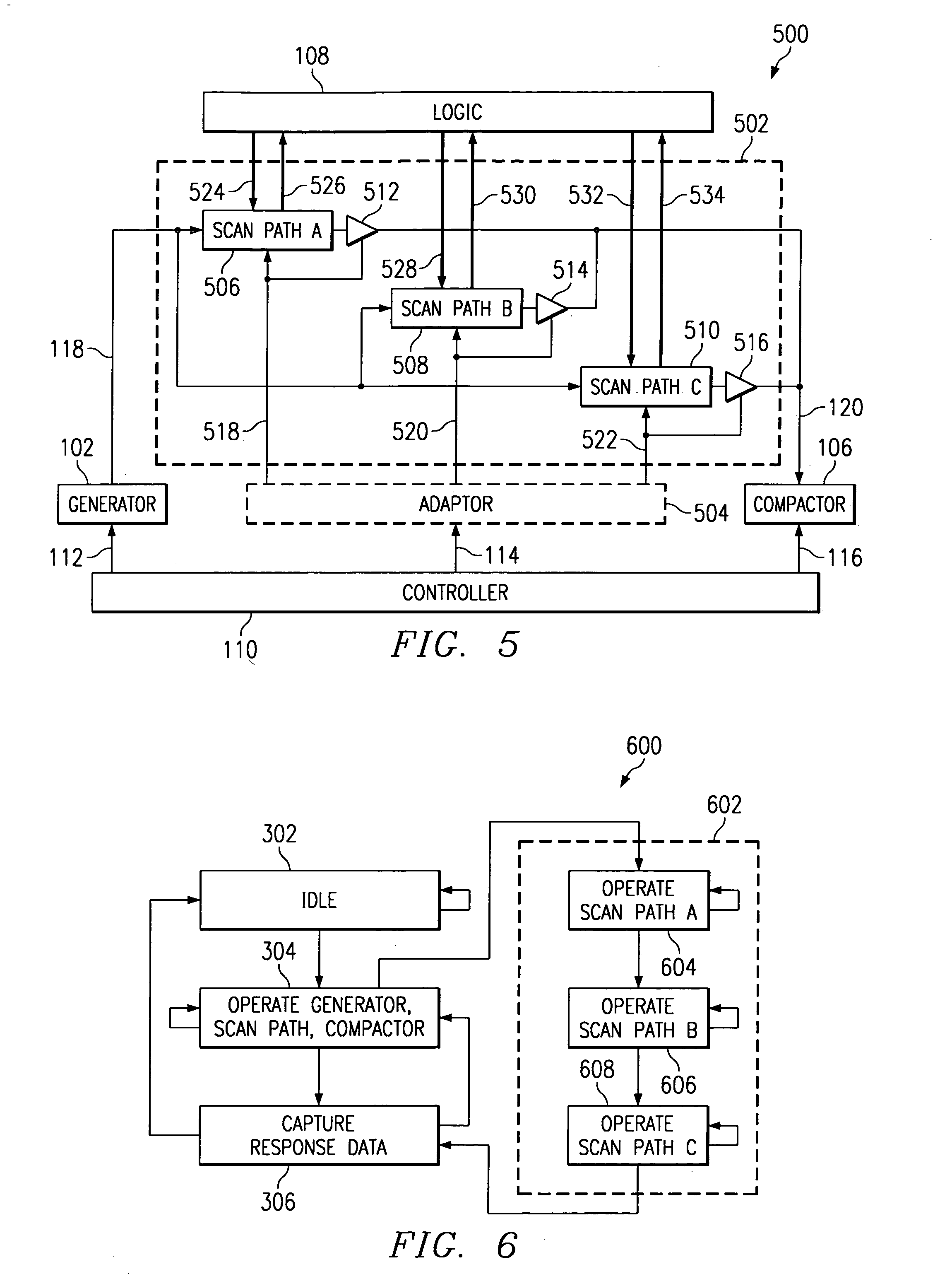
[0035]FIG. 5 illustrates the Scan-BIST architecture of FIG. 1 after it has been adapted into the low power Scan-BIST architecture of the present invention. In FIG. 5, it is seen that the generator 102, compactor 106, and controller 110 remain the same as in FIG. 1. The changes between the FIG. 1 Scan-BIST architecture and the FIG. 5 low power Scan-BIST architecture involve modification of scan path 104 into scan path 502, and the insertion of an adaptor circuit 504 in the control path 114 between controller 110 and scan path 502.

[0036] Adapting scan path 104 into scan path 502 involves reorganizing scan path 104 from being a single scan path containing all the scan cells (M), into a scan path having a desired number of selectable separate scan paths. In FIG. 5, scan path 502 is shown after having been reorganized into three separate scan paths A, B, and C 506-510. It is assumed at this point in the description that the number of scan cells (M) in scan path 104 is divisible by three...


PUM


Abstract

A Scan-BIST architecture is adapted into a low power Scan-BIST architecture. A generator 102, compactor 106, and controller 110 remain the same as in the known art. The changes between the known art Scan-BIST architecture and the low power Scan-BIST architecture involve modification of the known scan path into scan path 502, to insert scan paths A 506, B 508 and C 510, and the insertion of an adaptor circuit 504 in the control path 114 between controller 110 and scan path 502.

Description

[0001] The disclosure relates to and incorporates by reference TI patent specification TI-28085PS “Low Power Testing of Very Large Circuits”, and TI patent specification TI-30726 “Adapting Scan Architectures for Low Power Operation”. BACKGROUND OF THE INVENTION [0002] 1. Field of the Invention [0003] Scan-BIST architectures are commonly used to test digital circuitry in integrated circuits. The present invention describes a method of adapting conventional Scan-BIST architectures into low power Scan-BIST architectures. [0004] 2. Description of the Related Art [0005]FIG. 1 illustrates a conventional Scan-BIST architecture that a circuit 100 can be configured into during test. In the normal functional configuration, circuit 100 may be a functional sub-circuit within IC, but in test configuration it appears as shown in FIG. 1. The Scan-BIST architecture is typically realized within a sub-circuit of an IC, such as an intellectual property core DSP or CPU sub-circuit. The Scan-BIST archit...

Claims


Application Information

Patent Timeline
Patent Type & Authority Applications(United States)
IPC IPC(8): G01R31/28G01R31/317G01R31/3185
CPCG01R31/31721G01R31/3177G01R31/318575G01R31/318536G01R31/28G01R31/31723G01R31/31724
Inventor WHETSEL, LEE D.
Owner TEXAS INSTR INC
Why Eureka
Try Eureka