
Integrated circuit with inductor having horizontal magnetic flux lines

Active Publication Date: 2005-01-06
BELL SEMICON LLC
View PDF4 Cites 33 Cited by
  • Summary
  • Abstract
  • Description
  • Claims
  • Application Information

AI Technical Summary

Benefits of technology

[0011] The present invention involves an IC and a method of making an IC having at least one inductor that avoids the disadvantages described above. The geometry of the inductor minimizes the negative effects of the magnetic field thereof. Thus, there is no need for a guard ring to attenuate the magnetic field of the inductor. Additionally, other components of the IC can be placed in close proximity to the inductor without having to alter the margins in the design of either the inductor or the other components to account for the magnetic field of the inductor.

Problems solved by technology

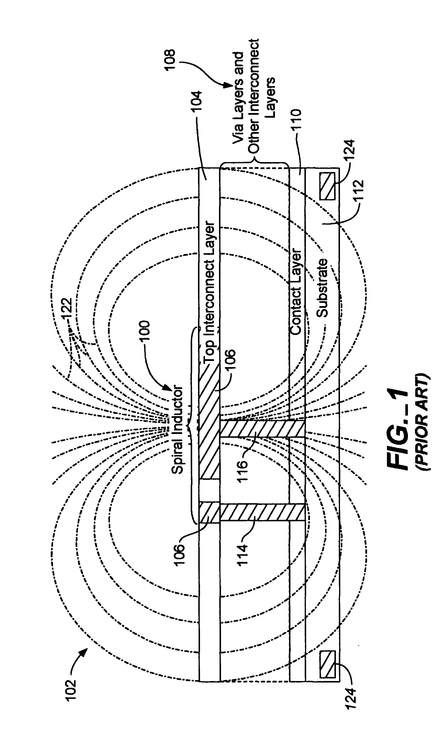
One aspect of IC's that affects the performance requirements and design margins is the interference between two components within the IC due to magnetic field generation by one or both of the components during operation of the IC.
For example, an inductor formed on an IC chip can generate a relatively strong time-dependent magnetic field, which can induce current in other parts, or circuitry, of the IC, thereby affecting the performance of the other parts of the IC.
Additionally, inductive coupling between the inductor and other parts of the IC, such as the substrate of the IC, can reduce the quality of the inductor, thereby affecting the performance of the inductor.
This option, however, takes up valuable space within the IC 102 and increases the cost of the IC 102.
This option, however, may waste valuable space in the IC 102 and require conductor lines between components to be undesirably long to reach between opposite sides of the inductor 100.
In fact, in some applications, the inductors may take up a significant percentage of the area of the IC, resulting in significantly fewer IC's per wafer if the other components cannot be placed close to the inductors.
This option, however, results in a lower-performing IC.
This option, however, results in a more expensive IC.
This option, however, may result in taking up a significant percentage of the IC's area with the inductors, increasing the size of the IC's and reducing the number of IC's per wafer.

Method used


Image

  • Integrated circuit with inductor having horizontal magnetic flux lines
  • Integrated circuit with inductor having horizontal magnetic flux lines
  • Integrated circuit with inductor having horizontal magnetic flux lines

Examples


Embodiment Construction

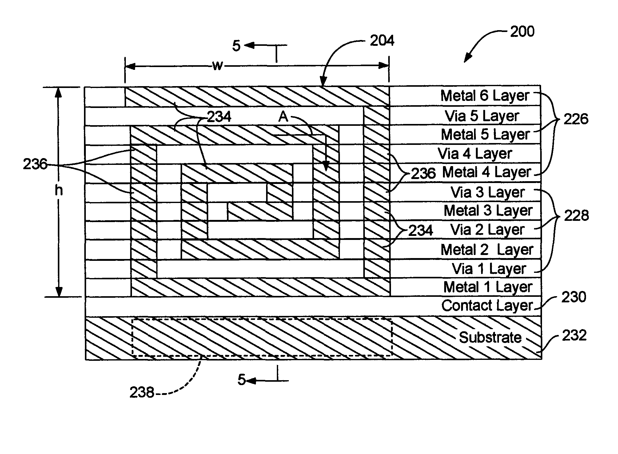
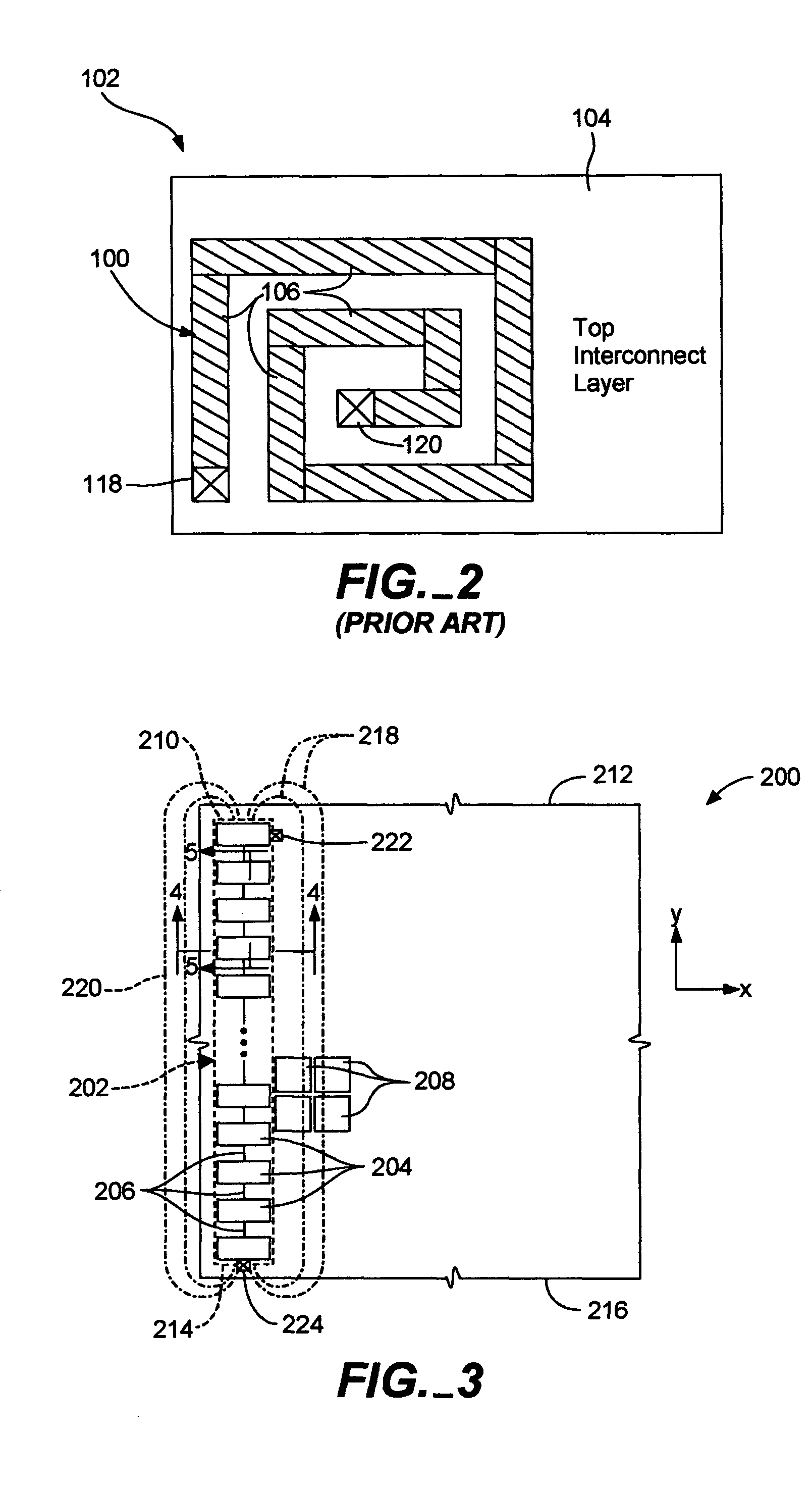
[0023] A portion of an integrated circuit (IC) 200, such as a mixed analog IC, which incorporates the present invention and which is formed by the methodology of the present invention is shown in FIG. 3. The IC 200 includes an inductor 202 formed by a plurality of inductor segments 204 connected by electrical conductors 206. Each segment 204 essentially forms one coil of the inductor 202, so the inductor 202 is effectively a coil-shaped inductor. The IC 200 also preferably includes a variety of other components 208, such as transistors, capacitors, resistors, etc. located throughout the IC 200, including adjacent (as shown) or under the inductor 202.

[0024] In a preferred embodiment, the inductor 202 is formed as shown with one end 210 located near an edge 212 of the IC 200 and an opposite end 214 of the inductor 202 located near an opposite edge 216 of the IC 200. In this configuration, a time-dependent magnetic field (indicated by magnetic flux lines 218) created by the inductor 2...


PUM


Abstract

An integrated circuit (IC) includes one or more inductors that have magnetic flux lines substantially parallel to a generally horizontal plane of the IC. The inductor is formed in a plurality of conductor layers separated by insulating layers of the IC. Regions of highest magnetic flux density of the inductor may preferably be located near the edge of the IC. Additionally, the inductor may preferably be segmented. The over-all inductance may preferably be controlled by turning on and off selected inductors or inductor segments.

Description

FIELD OF THE INVENTION [0001] This invention relates to semiconductor integrated circuits (ICs) having inductors formed therein. In particular, this invention relates to new and improved techniques for forming an inductor having horizontal, rather than vertical, magnetic flux lines within the IC. BACKGROUND OF THE INVENTION [0002] A significant trend throughout IC development has been to reduce the size of the components within the IC's. As the size is reduced, the performance requirements and design margins of the components become more stringent. One aspect of IC's that affects the performance requirements and design margins is the interference between two components within the IC due to magnetic field generation by one or both of the components during operation of the IC. For example, an inductor formed on an IC chip can generate a relatively strong time-dependent magnetic field, which can induce current in other parts, or circuitry, of the IC, thereby affecting the performance o...

Claims


Application Information

Patent Timeline
IPC IPC(8): H01L21/00H01L21/02H01L23/522
CPCH01L28/10H01L23/5227H01L2924/0002H01L2924/00
Inventor BHATT, HEMANSHU D.FURE, JANALLMAN, DERRYL D. J.
Owner BELL SEMICON LLC
Learn More