Optical element
a technology of optical elements and liquid crystal displays, applied in the field of optical elements, can solve the problems of large power consumption, low optical efficiency of conventional liquid crystal displays, and high power consumption
- Summary
- Abstract
- Description
- Claims
- Application Information
AI Technical Summary
Benefits of technology
Problems solved by technology
Method used
Image
Examples
example 1
[0057] A polyimide film (LX1400 (manufactured by Hitachi Chemical Co., Ltd., Japan)) with a thickness of 0.02 .mu.m was formed on a glass substrate. After baked at 250.degree. C., the polyimide film was then subjected to rubbing treatment for alignment.
[0058] The rubbed polyimide film on the glass substrate was spin-coated with a solution containing a cholesteric liquid crystal having a composition as described below.
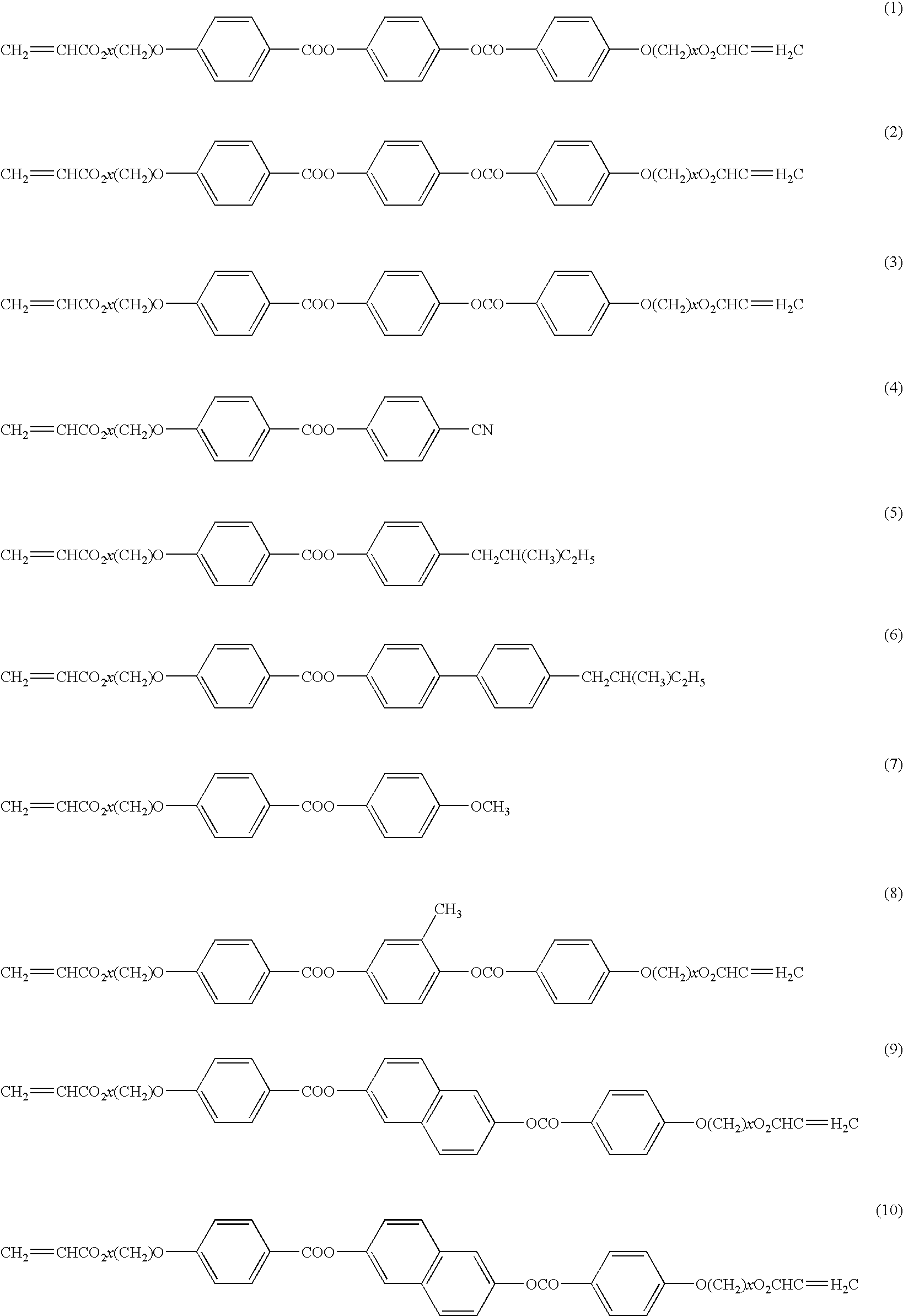
[0059] Nematic liquid crystal (above formula (8)): 95.45% by weight
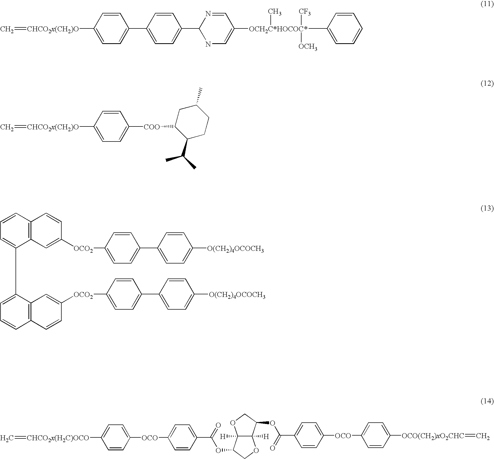
[0060] Chiral agent (above formula (14)): 4.55% by weight
[0061] Polymerization initiator (Irg907): 5% by weight
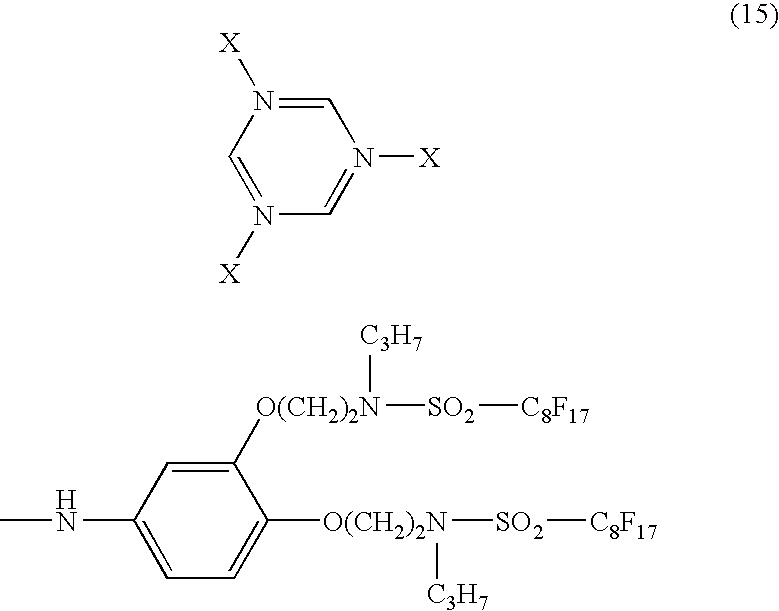
[0062] Surface active agent (below formula (15)): 0.05% by weight
[0063] Toluene: 175% by weight 3
[0064] As described above, the cholesteric liquid crystal solution contains a cholesteric liquid crystal (chiral nematic liquid crystal) which is a mixture of a nematic liquid crystal and a chiral agent.
[0065] The coating film applied to the polyimide film on the glass substrate was subjected to a tr...
example 2
[0069] An optical element was produced in the same manner as that of Example 1, other than that the thickness of the protective layer was made 1.5 .mu.m. The modulus of elasticity of thus obtained optical element according to Example 2 was determined by pushing, from the protective layer side, an indenter into the cholesteric liquid crystal layer with a test force of 2 mN in accordance with the universal hardness test method. As a result, the modulus of elasticity was 0.60, and the plastic deformation was 0.48 .mu.M. A protective layer was formed directly on a glass substrate in the same manner as that of Example 1, and its modulus of elasticity was determined by pushing an indenter into the protective layer with a test force of 2 mN in accordance with the universal hardness test method. As a result, the modulus of elasticity was found to be 0.60.
example 3
[0070] An optical element was produced in the same manner as that of Example 1, other than that JSS-341 (manufactured by JSR Corporation) was used as a material for forming a protective layer with its thickness being 1.5 .mu.m, and that the protective layer was not subjected to exposure process when forming the protective layer. The modulus of elasticity of thus obtained optical element according to Example 3 was determined by pushing, from the protective layer side, an indenter into the cholesteric liquid crystal layer with a test force of 2 mN in accordance with the universal hardness test method. As a result, the modulus of elasticity was 0.65, and the plastic deformation was 0.46 .mu.m. A protective layer was formed directly on a glass substrate in the same manner as that of Example 1, and its modulus of elasticity was determined by pushing an indenter into the protective layer with a test force of 2 mN in accordance with the universal hardness test method. As a result, the modu...
PUM
| Property | Measurement | Unit |
|---|---|---|
| indentation force | aaaaa | aaaaa |
| thickness | aaaaa | aaaaa |
| thickness | aaaaa | aaaaa |
Abstract
Description
Claims
Application Information
 - R&D
- Intellectual Property
- Life Sciences
- Materials
- Tech Scout
- Unparalleled Data Quality
- Higher Quality Content
- 60% Fewer Hallucinations
Browse by: Latest US Patents, China's latest patents, Technical Efficacy Thesaurus, Application Domain, Technology Topic, Popular Technical Reports.
© 2025 PatSnap. All rights reserved.Legal|Privacy policy|Modern Slavery Act Transparency Statement|Sitemap|About US| Contact US: help@patsnap.com


