
Wafer bias drive for plasma source

a plasma source and bias drive technology, applied in chemical/physical/physical-chemical processes, chemical discharge tubes, energy-based chemical/physical/physical-chemical processes, etc., can solve the problems of degrading the rf coupling of the workpiece and the plasma, the present tools for reactive ion etching have difficulty maintaining the process uniformity necessary, and the plasma used for processing is non-uniform

Inactive Publication Date: 2004-01-29
TOKYO ELECTRON LTD
View PDF17 Cites 45 Cited by
  • Summary
  • Abstract
  • Description
  • Claims
  • Application Information

AI Technical Summary

Benefits of technology

The present invention relates to a system for plasma processing that uses a segmented electrode for better control over the plasma processing. The system includes a segmented chuck with multiple sub-electrodes that are electrically isolated from each other. Each sub-electrode has its own RF driver for driving the sub-electrode. The system also includes a pin lift assembly for loading and unloading the workpiece. The use of a segmented chuck with internal or external power supplies and an optional optical sensor for measuring process data during plasma processing enables better control over the plasma processing and uniformity of the process. The invention provides a more uniform processing over larger wafers and larger silicon wafers.

Problems solved by technology

However, present tools for reactive ion etching have difficulty maintaining the process uniformity necessary even for today's requirements, which are substantially less stringent than those anticipated for the future.
The plasmas used for the processing, however, tend to be non-uniform, especially over large areas.
In general, however, systems with a segmented electrode avoid placement of a workpiece on the segmented electrode, and, as a result, the RF coupling of the workpiece with the plasma is degraded.
Typically these systems utilize a single RF source for driving the segments, possibly with phase differences, and so the ability to control the process to maintain uniformity is substantially limited.

Method used


Image

  • Wafer bias drive for plasma source
  • Wafer bias drive for plasma source
  • Wafer bias drive for plasma source

Examples


Embodiment Construction

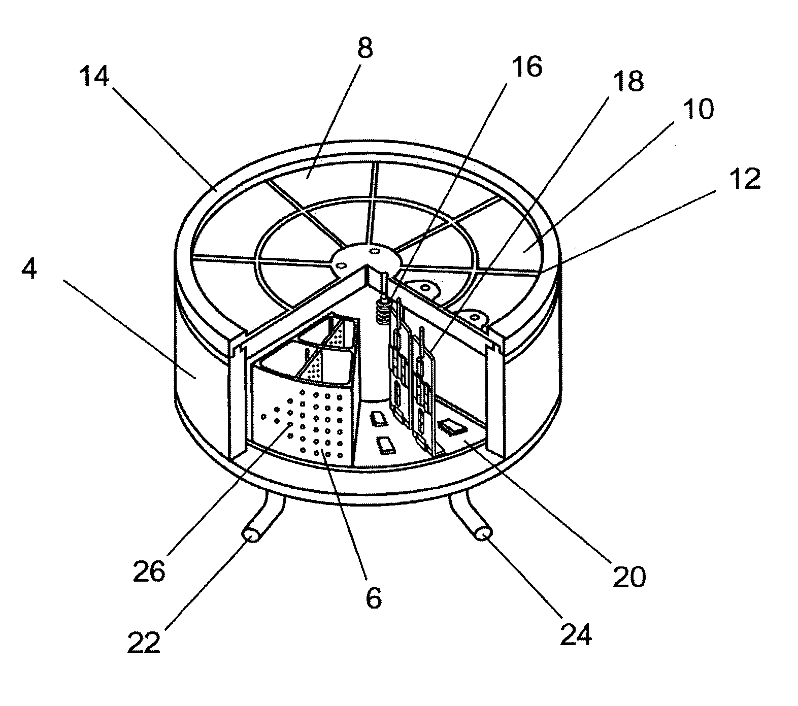
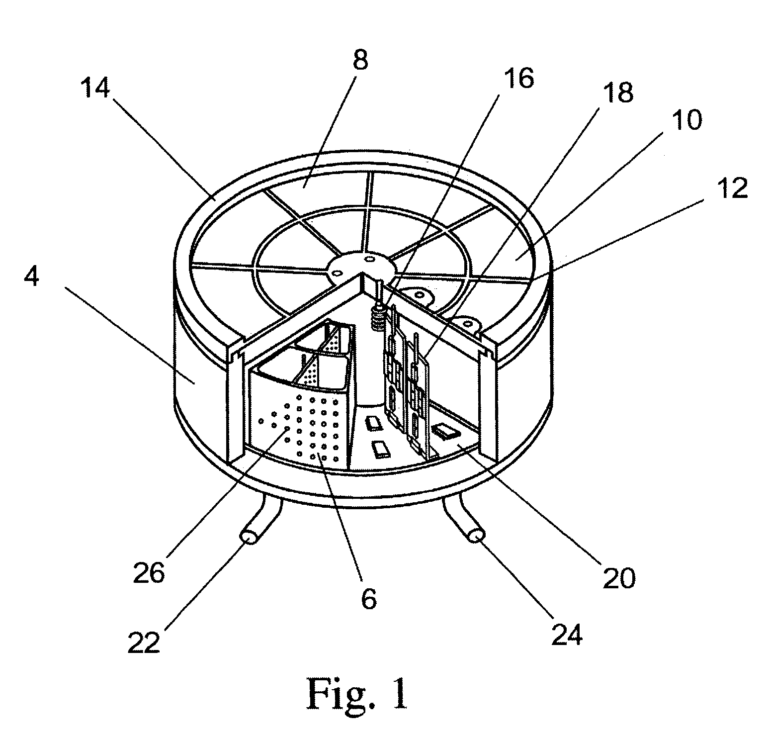
[0024] A segmented chuck 2 according to an embodiment of the present invention is shown in FIG. 1. The chuck 2 includes a chuck enclosure 4 that contains all of the chuck components. Additionally, an RF enclosure 6 provides for RF shielding of the chuck 2 and the components contained therein. A dielectric or semiconductor focus ring 14 is provided on the peripheral edge of the upper end of the chuck 2 as standard practice in plasma processing systems. The focus ring 14 consists of an insulating or semiconducting material suitably designed using conventional practices known in the art to aid with the plasma processing at the periphery of the workpiece placed on the chuck 2.

[0025] The chuck 2 includes a segmented electrode 8 with sixteen sub-electrodes 10; however, any suitable subdivision may be employed. Insulators 12 are provided between the sub-electrodes 10 to provide electrical isolation so that the sub-electrodes can be independently driven. The insulator between electrodes can...


PUM


Abstract

A segmented chuck provides uniform processing of a workpiece (e.g., a wafer) with a plasma in a process chamber. The segmented chuck includes a segmented electrode having a plurality of sub-electrodes where the sub-electrodes are electrically isolated from one another by insulating connections and the segmented electrode defines a process surface that is adapted to receive the workpiece. The segmented chuck also includes a plurality of RF drivers for driving the sub-electrodes with RF biases, where the RF biases couple the workpiece with the plasma in the process chamber. By allowing the workpiece to be placed on the chuck, the coupling between the plasma and the workpiece is enhanced. By allowing the sub-electrodes to be independently driven by RF drivers, more uniform processing can be achieved with larger workpieces.

Description

[0001] This is a continuation of International Application No. PCT / US01 / 51642, filed on Dec. 2, 2001, and which, in turn, claims benefit of U.S. Provisional Application, No. 60 / 256,387, filed Dec. 19, 2000, the contents of both of which are incorporated herein in their entirety.[0002] 1. Field of Invention[0003] The present invention relates to plasma processing and more particularly to a system having a segmented electrode for use in plasma processing.[0004] 2. Description of Related Art[0005] As the dimensions of the features in Integrated Circuits (IC's) have shrunk over recent years, the requirements for uniformity of processing have tightened significantly. At the same time, the nominal size of a wafer has grown from 6 inches in diameter to 8 inches and is currently reaching 12 inches (300 mm). As a result, the requirements for tighter process uniformity must be maintained over a significantly larger area. However, present tools for reactive ion etching have difficulty maintain...

Claims


Application Information

Patent Timeline
Patent Type & Authority Applications(United States)
IPC IPC(8): H01J37/32H01L21/00H01L21/683
CPCH01J37/32009H01J37/32532H01L21/6838H01L21/67069H01J37/32706
Inventor LONG, MAOLINPARSONS, RICHARDJOHNSON, WAYNE L.
Owner TOKYO ELECTRON LTD
Learn More