Punched adhesive tape for semiconductor, method of manufacturing lead frame with the adhesive tape, lead frame with the adhesive tape, and semiconductor device comprising the lead frame

Inactive Publication Date: 2003-01-30
HITACHI CHEM CO LTD
View PDF11 Cites 7 Cited by
  • Summary
  • Abstract
  • Description
  • Claims
  • Application Information

AI Technical Summary

Benefits of technology

[0006] The object of the present invention is to solve the above problems and to provide an adhesive tape for semiconductor which is excellent in work efficiency, a method of producing an adhesive tape-bearing lead frame using the same, an adhesive tape-bearing lead frame, and a semiconductor device fabricated by using the same. As a result of study to prevent contamination without cutting adhesive tapes nor contaminating them by marking with seals or ink, we have hit upon an idea that punching adhesive tapes at or in the vicinity of the regions containing contaminants or defects is excellent in work efficiency and overcomes the above problems, and we have consequently completed the present invention.
[0016] Exemplary films usable as the base film in the present invention include insulating heat resistant resin films, such as polyimide films, polyether-amide films, polyether-amide-imide films, polyether-sulfone films, polyether-ether-ketone films and polycarbonate films. The base film is preferably transparent. The thickness of the base film is preferably 5 to 200 .mu.m, more preferably 25 to 50 .mu.m. Base films thicker than 200 .mu.m are disadvantageous to the production of thin resin-molded semiconductor devices, and base films thinner than 5 .mu.m may lower the work efficiency in adhesive coating.
[0032] Preferably, the method of the present invention for producing an adhesive tape-bearing lead frame by using a punched adhesive tape for semiconductor is carried out by employing a common process for applying adhesive tapes to lead frames which comprises unwinding an adhesive tape, punching the adhesive tape (to punch out an adhesive tape piece to be applied to a lead frame), applying the adhesive tape piece, and winding the punched adhesive tape, and by adding thereto a step of detecting punched holes prior to the punching of the adhesive tape piece. The detection of punched holes can be carried out visually, but preferably by using a CCD camera, which permits automatic detection and improves the work efficiency.
[0033] By winding (skipping) the punched adhesive tape for semiconductor a certain length, for example .+-.20 cm, preferably .+-.10 cm from the center of each punched hole in the direction of the length of the punched adhesive tape for semiconductor without punching the regions containing the detected punched holes, it can be prevented to apply adhesive tape pieces containing contaminants or defects to lead frames. Further, since the regions of the material adhesive tape where contaminants or defects are contained are marked by punching, there is no fear of contaminating semiconductor chips due to external causes, for example, due to the marking of contaminants and defects with seals or ink. The method of the present invention also reduces the work time since it permits using long adhesive tapes as they are without cutting, thereby reducing the number of the exchanges of adhesive tapes during the work for applying adhesive tape pieces. That is, according to the method of the present invention, adhesive tape-bearing lead frames can be produced efficiently with good yield.
[0034] The obtained adhesive tape-bearing lead frame has an advantage of low production cost since the use of the punched adhesive tape for semiconductor of the present invention improves the work efficiency, yield and productivity in the production of the adhesive tape-bearing lead frame. Also, the adhesive tape-bearing lead frame can decrease defects in the semiconductor devices produced using them, reducing the production cost.

Problems solved by technology

This method however requires many hands and is inefficient.
This method also needs improvement since the adhesive tapes may be contaminated by the marking, causing the contamination of adherend chips.

Method used


Image

  • Punched adhesive tape for semiconductor, method of manufacturing lead frame with the adhesive tape, lead frame with the adhesive tape, and semiconductor device comprising the lead frame
  • Punched adhesive tape for semiconductor, method of manufacturing lead frame with the adhesive tape, lead frame with the adhesive tape, and semiconductor device comprising the lead frame

Examples


example 2

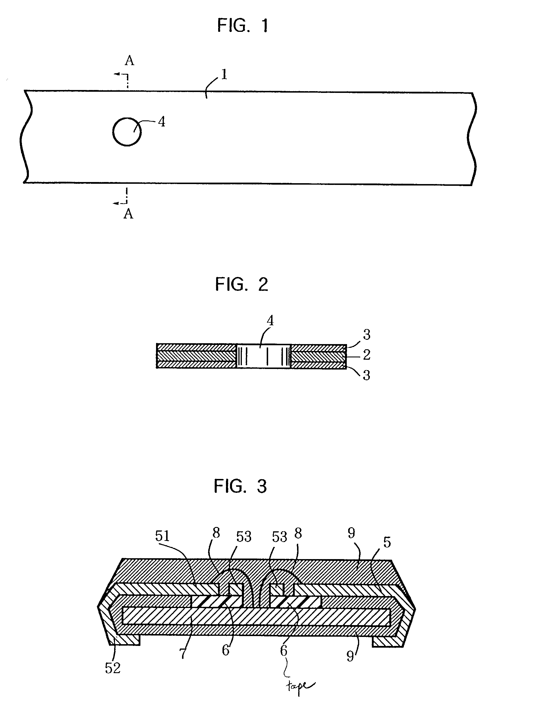
[0039] An adhesive tape (trade name: HM-122U, produced by Hitachi Chemical Company, Ltd.) 50 m long by 9 mm wide was subjected to an appearance inspection using a contaminant (defect) inspector consisting of an adhesive tape-unwinding part, a CCD camera, a punching part and an adhesive tape-winding part. In the course of the inspection, the contaminated or defective parts detected by the CCD camera or the neighborhoods thereof were punched out (punched hole: a circular hole of 3 mm in diameter) at the punching part. Thus a punched adhesive tape for semiconductor 50 m long was obtained without cutting the adhesive tape.

example 3

[0040] An adhesive tape (trade name: HM-122U, produced by Hitachi Chemical Company, Ltd.) 300 m long by 9 mm wide was subjected to an appearance inspection using a contaminant (defect) inspector consisting of an adhesive tape-unwinding part, a CCD camera, a punching part and an adhesive tape-winding part. In the course of the inspection, the contaminated or defective parts detected by the CCD camera or the neighborhoods thereof were punched out (punched hole: a circular hole of 3 mm in diameter) at the punching part. Thus a punched adhesive tape for semiconductor 300 m long was obtained without cutting the adhesive tape.

example 4

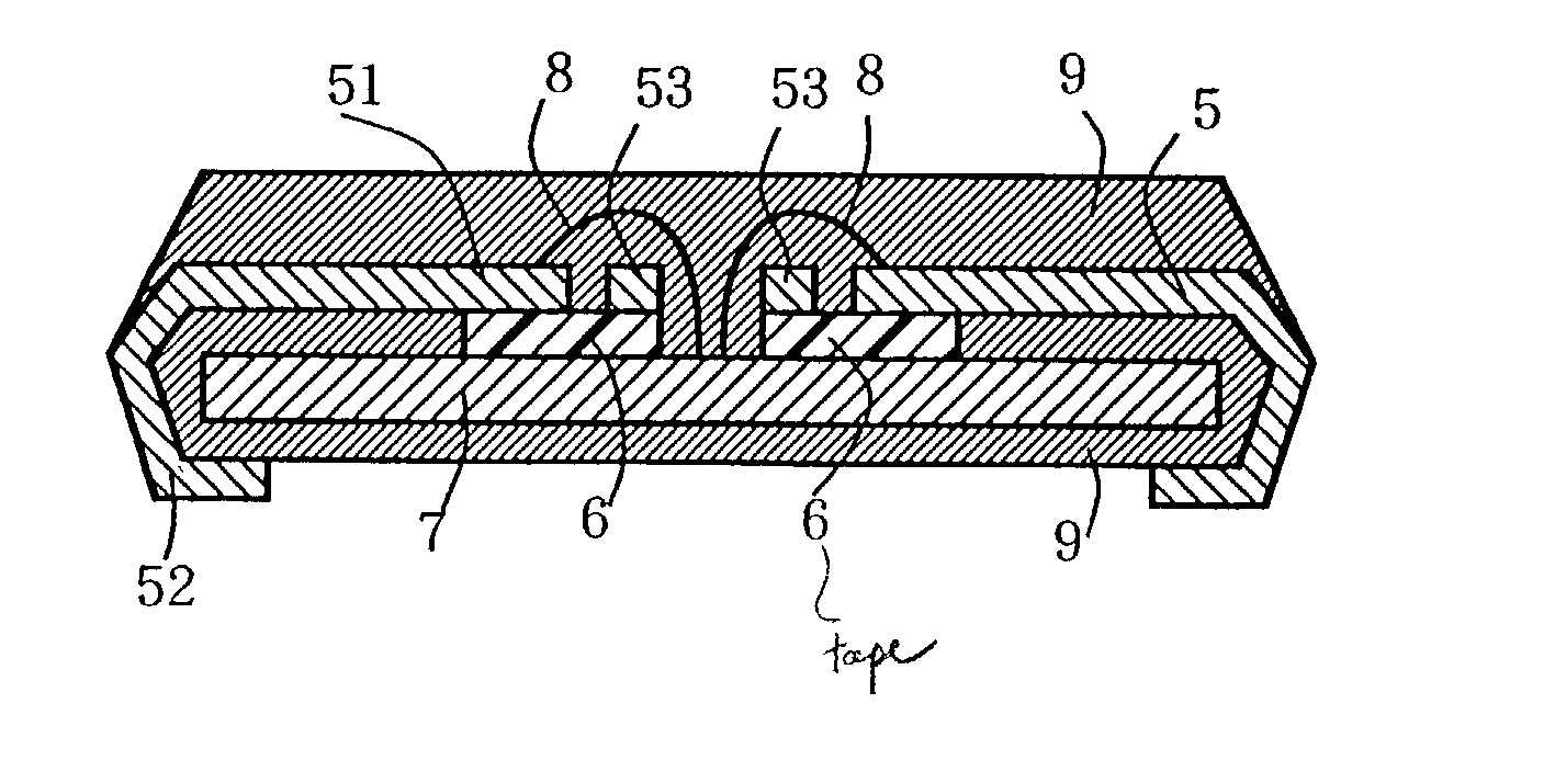
[0041] Using the punched adhesive tape for semiconductor produced in Example 1, an adhesive tape-bearing lead frame was produced as follows. A 42 alloy lead frame comprising inner leads, outer leads and bus bars was used, and adhesive tape pieces (1 mm.times.6 mm) were applied to the inner leads and bus bars by a continuous process comprising unwinding the adhesive tape, detecting punched holes, punching out adhesive tape pieces, applying them to the lead frame, and winding the adhesive tape, wherein the adhesive tape pieces punched out from the adhesive tape for semiconductor were applied to the lead frame by pressing them to the lead frame at 400.degree. C. for 3 seconds under a pressure of 3 MPa. The detection of punched holes were carried out using a CCD camera, and on detection of each punched hole, the adhesive tape was wound by 10 cm in the direction of length without punching, to avoid punching a part of a length of .+-.5 cm from the center of the punched hole in the directi...


PUM

PropertyMeasurementUnit
Diameteraaaaaaaaaa
Thicknessaaaaaaaaaa
Electrical resistanceaaaaaaaaaa

Abstract

A punched adhesive tape for semiconductor which is made by punching an adhesive tape comprising a base film and an adhesive layer provided on one or each side of the base film to mark the regions in the adhesive tape where contaminants or defects are contained; a method of producing an adhesive tape-bearing lead frame by punching the punched adhesive tape for semiconductor, with the parts containing the punched holes skipped over, and applying the adhesive tape pieces punched out from the punched adhesive tape for semiconductor to a lead frame; a semiconductor device fabricated by using the adhesive-bearing lead frame.

Description

[0001] The present invention relates to punched adhesive tapes for semiconductor particularly suitable for use in semiconductor devices wherein semiconductor elements (chips) are bonded to lead frames, and also relates to the production of adhesive tape-bearing lead frames, to adhesive tape-bearing lead frames and to semiconductor devices fabricated using the adhesive tape-bearing lead frames.[0002] In resin-molded semiconductor devices, adhesive tapes are now mainly used as the adhesives for bonding semiconductor elements (chips) to lead frames.[0003] If the adhesive tapes used for the above purpose contain contaminants or defects, the reliability of semiconductor devices may be lowered. It is therefore necessary to inspect adhesive tapes for contaminants and defects before applying the adhesive tapes to adherend lead frames, to avoid using adhesive tapes containing contaminants or defects.[0004] A conventional, simple method of removing contaminants is to cut off the parts contain...

Claims


Application Information

Patent Timeline
IPC IPC(8): H01L23/495H01L23/544
CPCH01L23/4951Y10T156/1084H01L2223/54473H01L2224/32014H01L2224/48091H01L2224/48247H01L2224/4826H01L2224/73215H01L2224/73253H01L2224/83856H01L2924/01005H01L2924/01027H01L2924/01029H01L2924/01033H01L2924/01077H01L2924/01079H01L2924/01082H01L23/544Y10T156/1062Y10T428/28Y10T428/2852Y10T428/24273Y10T428/24322Y10T156/1056H01L2224/83192H01L2224/83101H01L24/45H01L24/29H01L24/27H01L2224/32245Y10S428/901H01L24/32H01L24/48H01L2924/01006H01L2924/01075H01L2224/45144H01L2924/00014H01L2924/00012H01L2924/00H01L2924/181Y10T83/9416Y10T83/155Y10T83/543H01L2224/2612H01L23/50
Inventor TANABE, YOSHIYUKINOMURA, YOSHIHIROKIRIHARA, HIROSHIHOSOKAWA, YOUICHIIIOKA, SHINJIYANAGISAWA, SATORU
Owner HITACHI CHEM CO LTD
Why Eureka
Try Eureka