Antenna element
a technology of antenna elements and elements, applied in the structural form of radiating elements, leaky waveguide antennas, resonance antennas, etc., can solve the problems of disturbance of radiation characteristic of radiation elements, unsuitable for miniaturization, and techniques that contradict miniaturization, and achieve enhanced radiation efficiency and bandwidth of radiation elements, stable characteristics
- Summary
- Abstract
- Description
- Claims
- Application Information
AI Technical Summary
Benefits of technology
Problems solved by technology
Method used
Image

Examples
experiment 1
[0106] Experiment 1
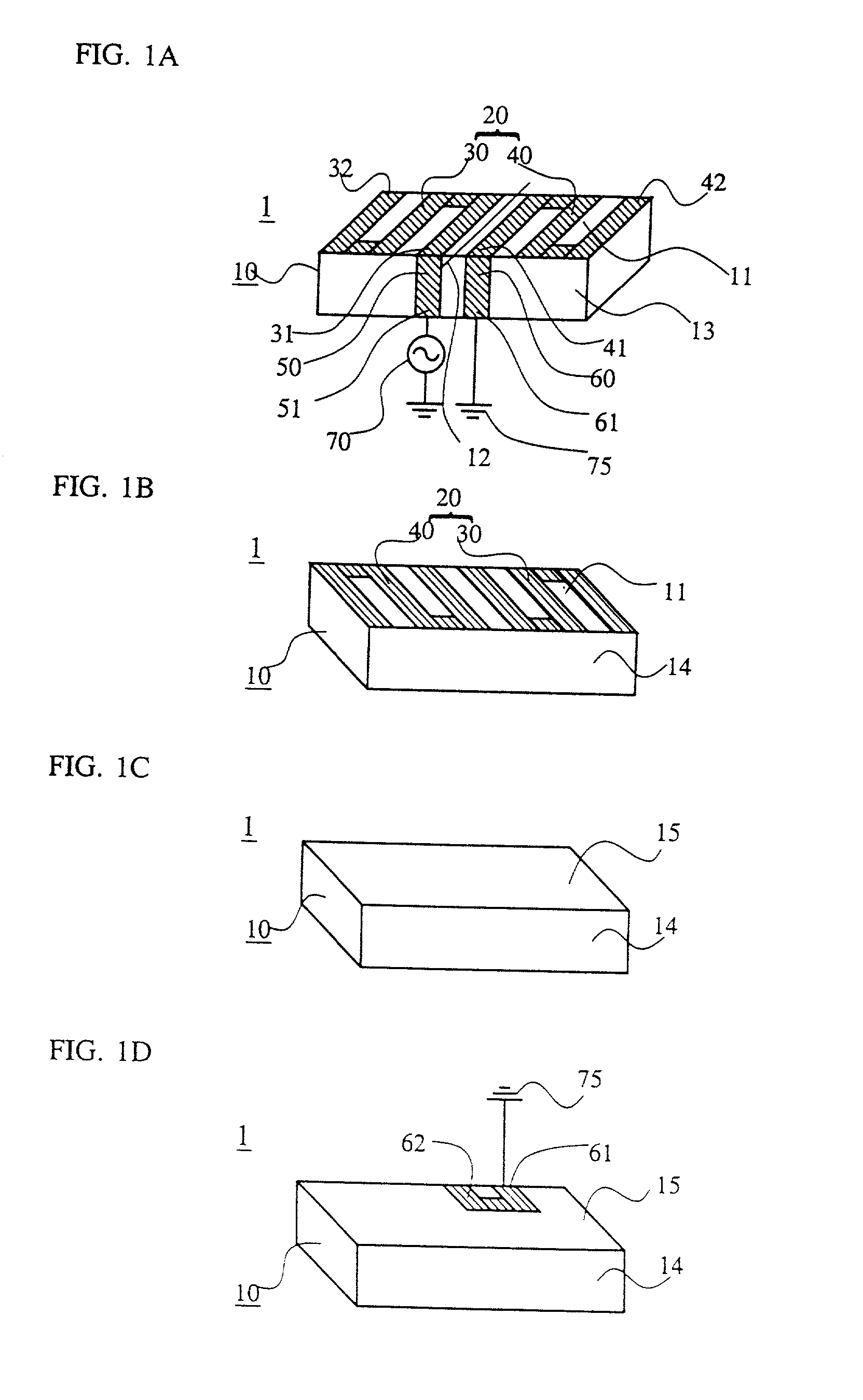
[0107] The antenna element 2 shown in FIG. 3 was fabricated and the reflection loss and the voltage standing wave ratio (VSWR) thereof was measured. Using a dielectric having a dielectric constant .epsilon.r of 40, and tan .delta. of 0.0002, a hexahedron substrate 10 of 3.0 mm wide, 13.4 mm long, and 1.5 mm thick was prepared. The halves 30a, 40a of the meandering radiation electrode 20a was provided on the top surface 11 and the rear surface 14 so that the respective halves has a length of a quarter of the radiation wavelength. Here again, reference numerals 13 and 15 denotes the front surface and the bottom surface of the substrate 10, respectively. The widths of the respective conductors were, from the outer side toward the center, 0.40 mm, 0.45 mm, 0.50 mm, 0.55 mm, 0.60 mm, 0.65 mm, and 0.70 mm, and the heights (vertical widths in the drawing) of the folded portions were, from the outer side toward the center, 0.40 mm, 0.45 mm, 0.50 mm, 0.55 mm, 0.60 mm, and ...
experiment 2
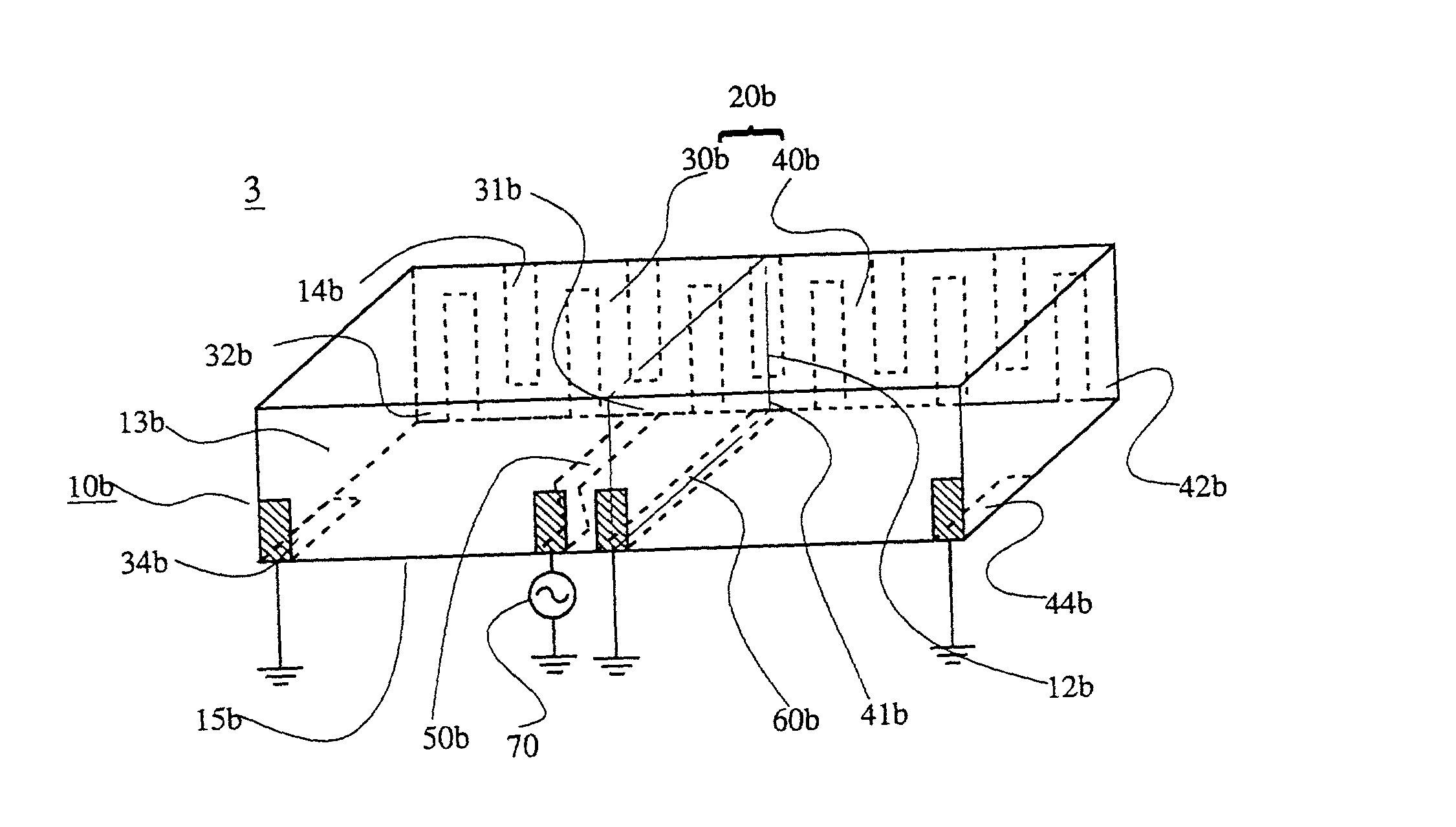
[0109] Experiment 2
[0110] The antenna element 3 shown in FIG. 4 was fabricated and the voltage standing wave ratio (VSWR) thereof was measured. Using a dielectric having a dielectric constant .epsilon.r of 40, and tan 6 of 0.0002, a hexahedron substrate of 3.0 mm wide, 10 mm long, and 2 mm thick was prepared. FIG. 21 is a developed view of only conductors including the antenna element 20b, the ground conductor 82 of the printed wiring board 80, and conductors and leads for connecting them. In this drawing, the rear surface 14b and the bottom surface 15b of the dielectric substrate 10b, and the ground conductor area 82 of the printed wiring board 80 are shown in this order from top to bottom. The both halves of the radiation electrode 20b were meandering quarter-wave antennas. The width of the conductor of the radiation electrode was 0.60 mm, and the gap width between the conductors was 0.60 mm. The antenna element 2 was mounted on the printed wiring board 80 in such a manner that th...
PUM
 Abstract
Description
Claims
Application Information
 - R&D
- Intellectual Property
- Life Sciences
- Materials
- Tech Scout
- Unparalleled Data Quality
- Higher Quality Content
- 60% Fewer Hallucinations
Browse by: Latest US Patents, China's latest patents, Technical Efficacy Thesaurus, Application Domain, Technology Topic, Popular Technical Reports.
© 2025 PatSnap. All rights reserved.Legal|Privacy policy|Modern Slavery Act Transparency Statement|Sitemap|About US| Contact US: help@patsnap.com