
Semiconductor wafer processing system with vertically-stacked process chambers and single-axis dual-wafer transfer system

a technology of process chambers and semiconductors, applied in the direction of conveyor parts, transportation and packaging, coatings, etc., can solve the problems of short mean time between failures, high apparatus cost, slow wafer processing,

Inactive Publication Date: 2002-03-21
AVIZA TECHNOLOGY INC
View PDF6 Cites 80 Cited by
  • Summary
  • Abstract
  • Description
  • Claims
  • Application Information

AI Technical Summary

Benefits of technology

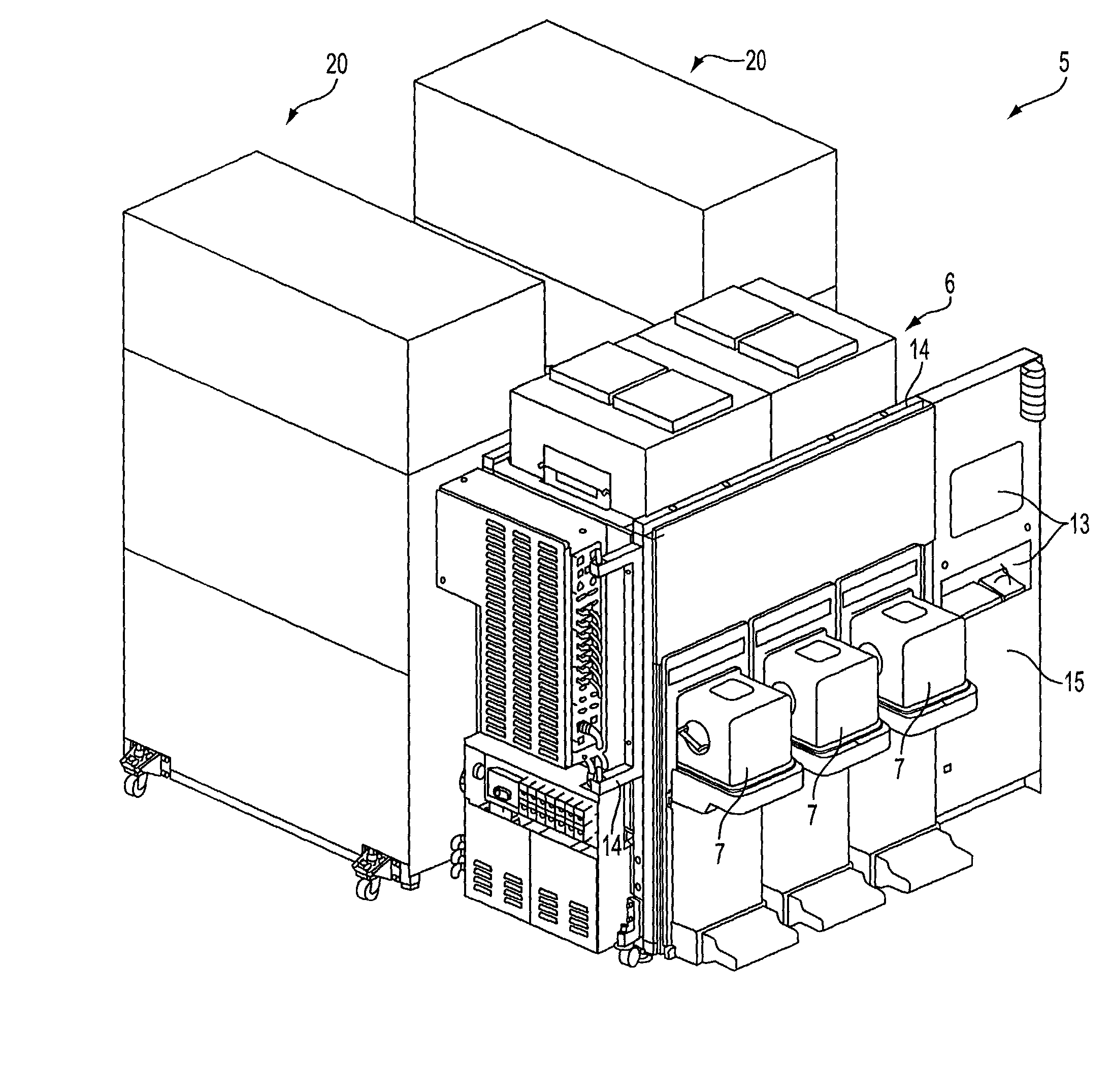
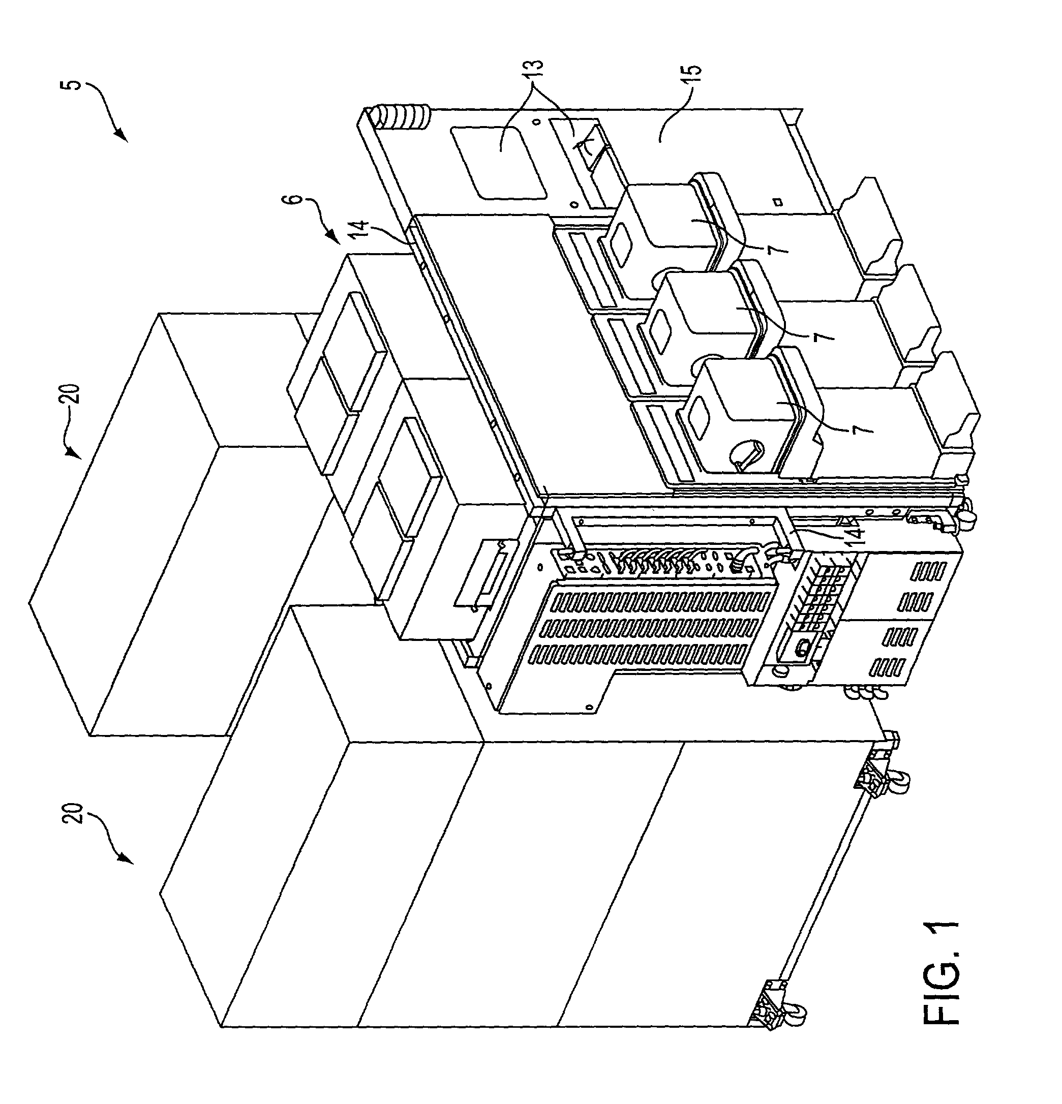
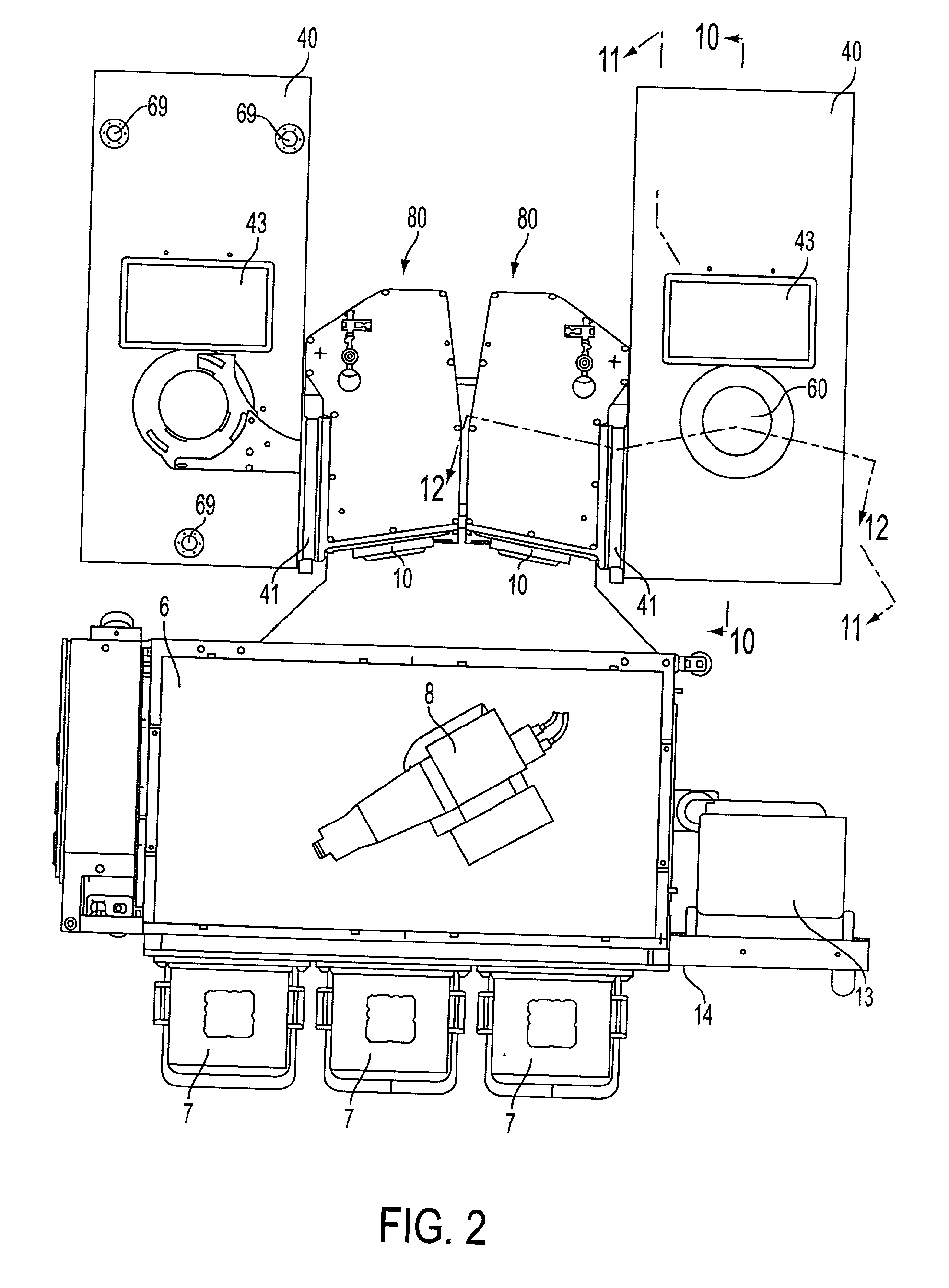
[0019] It is an object of the present invention to vertically stack two or more loadlock-process chamber assemblies to form a multi-chamber module in order to reduce the system footprint and thus optimize the vertical orientation and layout of the loadlock-process chamber assembly stacks.
[0022] It is another object of the present invention to optimize wafer flow paths and process timing for a linear array, vertically-stacked processing system and method in order to maximize throughput of each process chamber and of the full processing system.
[0023] It is another object of the present invention to optimize the number of process chambers within a footprint to increase processing system throughput.
[0025] It is another object of the present invention to provide a transfer arm having the capacity to carry two wafers in order to facilitate and expedite wafer transfer between the loadlock chamber and the process chamber. In particular, it is an object of the present invention to provide a transfer arm which has the capacity to carry an unprocessed wafer and a processed wafer at the same time in order to maximize system throughput.
[0026] It is another object of the present invention to provide a wafer cooling plate to reduce wafer cooling time after a wafer is processed to facilitate wafer transfer out of the loadlock and into a cassette maximizing parallel steps within the processing system and thus increasing throughput of the processing system.

Problems solved by technology

The complexity of the machinery has resulted in high cost of the apparatus, slow wafer processing and a short mean time between failures.
Although the loading chambers and the treatment chambers appear to be stacked in a vertical direction, the pressure gas system and vacuum system are horizontally disposed from the treatment chambers and thus disadvantageously increases the footprint of the reaction furnace.
Although the process units may be vertically stacked, only one main handler is provided for transferring substrates to each of the process units, whereby the throughput of each process unit cannot be maximized.
However, as indicated in FIG. 4, the scheduling can be quite complex.
However, the addition of a cooling chamber or a position where the wafer must "wait" and cool further complicates the scheduling of wafers moved by the central hub robot, and thus also complicates the scheduling of the central hub robot with respect to that of the front end robot.
Often, in practice, even the slightest pause in wafer transfer to one process chamber (or loadlock) can disrupt overall wafer flow throughout the whole system.
Schedulers may purposely include slight delays in scheduling programs to accommodate these slight potential delays at the cost of less than optimal throughput.
In short, synchronization between the two robots that must choose among several multi-accessible wafer locations, including the load cassettes, loadlocks, and process chambers, is key to maintaining acceptable throughput, but such synchronization is very complex.
One should appreciate that individual delivery systems, for example individual flow control valves, may instead be utilized for each process chamber but such configuration may result in higher costs.

Method used


Image

  • Semiconductor wafer processing system with vertically-stacked process chambers and single-axis dual-wafer transfer system
  • Semiconductor wafer processing system with vertically-stacked process chambers and single-axis dual-wafer transfer system
  • Semiconductor wafer processing system with vertically-stacked process chambers and single-axis dual-wafer transfer system

Examples


Embodiment Construction

[0086] Referring particularly to FIGS. 16(a)-(l), an exemplary method of semiconductor wafer transfer and processing in accordance with the present invention is schematically illustrated in which a loadlock chamber 80 is attached to a respective process chamber 40. A loadlock transfer arm (not shown in FIG. 16) similar to transfer arm 83 receives semiconductor wafers from a front end robot 8 (not shown in FIG. 16) moves the wafers between the loadlock chamber and the process chamber.

[0087] Three tiers illustrated within loadlock chamber 80 represent wafer positions when resting on upper wafer shelf 85', lower wafer shelf 87', and cooling plate 95' within loadlock chamber 80. A fourth "pins up" wafer position slightly above the cooling plate is not shown, but is discussed below. Two tiers illustrated within process chamber 40 represent wafer positions when the wafer is resting on upper wafer shelf 85" and lower wafer shelf 87" within process chamber 40. Other wafer positions such as ...


PUM

PropertyMeasurementUnit
vacuum pressuresaaaaaaaaaa

Abstract

A semiconductor wafer processing system including a multi-chamber module having vertically-stacked semiconductor wafer process chambers and a loadlock chamber dedicated to each semiconductor wafer process chamber. Each process chamber includes a chuck for holding a wafer during wafer processing. The multi-chamber modules may be oriented in a linear array. The system further includes an apparatus having a dual-wafer single-axis transfer arm including a monolithic arm pivotally mounted within said loadlock chamber about a single pivot axis. The apparatus is adapted to carry two wafers, one unprocessed and one processed, simultaneously between the loadlock chamber and the process chamber. A method utilizing the disclosed system is also provided.

Description

[0001] This application claims priority to U.S. Provisional Patent Application Serial No. 60 / 127,532 filed Apr. 2, 1999, entitled NEAR ATMOSPHERIC CVD SYSTEM WITH VERTICALLY-STACKED PROCESS CHAMBERS.[0002] This application also claims priority to U.S. Provisional Patent Application Serial No. 60 / 127,650 filed Apr. 2, 1999, entitled SINGLE-AXIS DUAL-WAFER TRANSFER SYSTEM.[0003] 1. Field of the Invention[0004] This invention relates generally to semiconductor wafer processing systems, apparatuses, and methods. In particular, the present invention relates to a structure with vertically-stacked process chambers which minimize the footprint while maximizing throughput of a semiconductor wafer processing system. For example, the present invention may be used to translate wafers within a near-atmospheric chemical vapor deposition (CVD) system, a rapid thermal oxidation system, or other types of wafer processing systems. The invention also particularly relates to a wafer transfer apparatus ...

Claims


Application Information

Patent Timeline
Patent Type & Authority Applications(United States)
IPC IPC(8): G03F7/20C23C16/54H01L21/00H01L21/02H01L21/31H01L21/677H01L21/687
CPCC23C16/54H01L21/67173H01L21/67178H01L21/6719H01L21/67196Y10S414/141H01L21/67742H01L21/67745H01L21/67751H01L21/68707H01L21/67201
Inventor SAVAGE, RICHARD N.MENAGH, FRANK S.CARVALHEIRA, HELDER R.TROIANI, PHILIP A.COSSENTINE, DAN L.VAUGHAN, ERIC R.MAYER, BRUCE E.
Owner AVIZA TECHNOLOGY INC
Learn More