
Address generator of dynamic memory testing circuit and address generating method thereof

a dynamic memory and address generator technology, applied in the field of testing a memory, can solve the problems of increasing the size and complexity of the circuit, hard to optimize the area of such devices, and increasing the difficulty in optimizing the area of bist circuit including the address generator

Inactive Publication Date: 2001-12-06
SAMSUNG ELECTRONICS CO LTD
View PDF0 Cites 8 Cited by
  • Summary
  • Abstract
  • Description
  • Claims
  • Application Information

AI Technical Summary

Benefits of technology

[0019] The invention can operate to generate testing addresses in the desired order and using only the selected portions of addresses using only a single counter, either an up counter or a down counter. Because only a single counter is used, significant savings in counter circuit size and complexity can be realized. In addition, because only a single counter can be used, the associated controlling circuitry is also smaller and less complex and, therefore, less costly to develop and manufacture.

Problems solved by technology

Accordingly, it is hard to optimize the area of such devices.
This additional circuitry adds to the difficulty in optimizing the area of the BIST circuit including the address generator.
This also greatly increases circuit size and complexity.
Also, the hardware of the BIST controlling portion for controlling the up / down counter or the up and down counters can be very large and complex.

Method used


Image

  • Address generator of dynamic memory testing circuit and address generating method thereof
  • Address generator of dynamic memory testing circuit and address generating method thereof
  • Address generator of dynamic memory testing circuit and address generating method thereof

Examples


Embodiment Construction

)

[0028] Hereinafter, the configuration and operation of a DRAM BIST circuit which uses an address generator according to the present invention and an address generating method thereof will be described with reference to the attached drawing s.

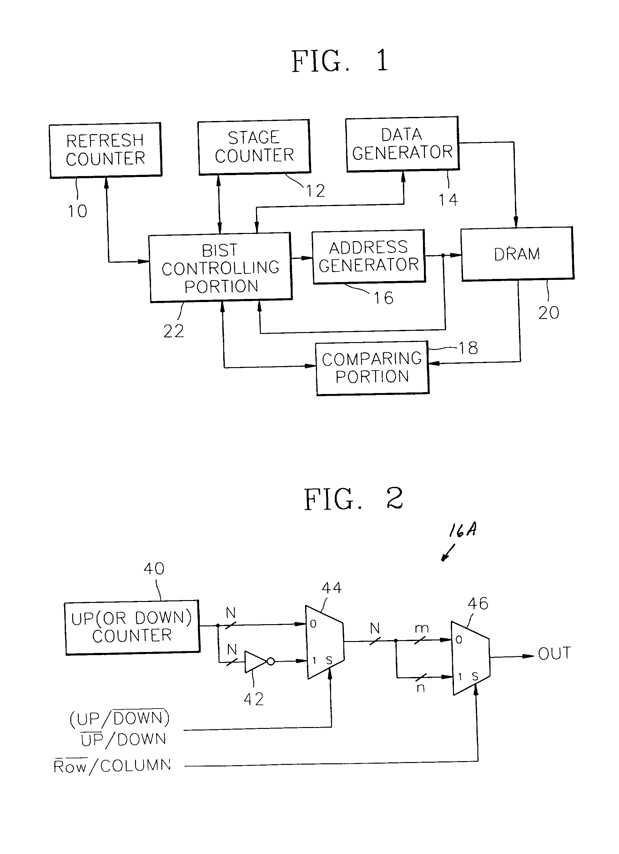
[0029] Referring to FIG. 1, a general DRAM BIST circuit includes a refresh counter 10, a stage counter 12, a data generating portion 14, an address generating portion 16, a comparing portion 18, and a BIST controlling portion 22. The refresh counter 10 determines a refresh timing of a DRAM 20. The stage counter 12 counts the respective steps of a memory testing method which proceeds by increasing or decreasing the memory addresses. The counter 12 outputs the counted result to the address generating portion 16 through the BIST controlling portion 22.

[0030] The data generating portion 14 generates data to be written in the DRAM 20 and outputs reference data to the comparing portion 18 through the BIST controlling portion 22. The BIST controlling ...


PUM


Abstract

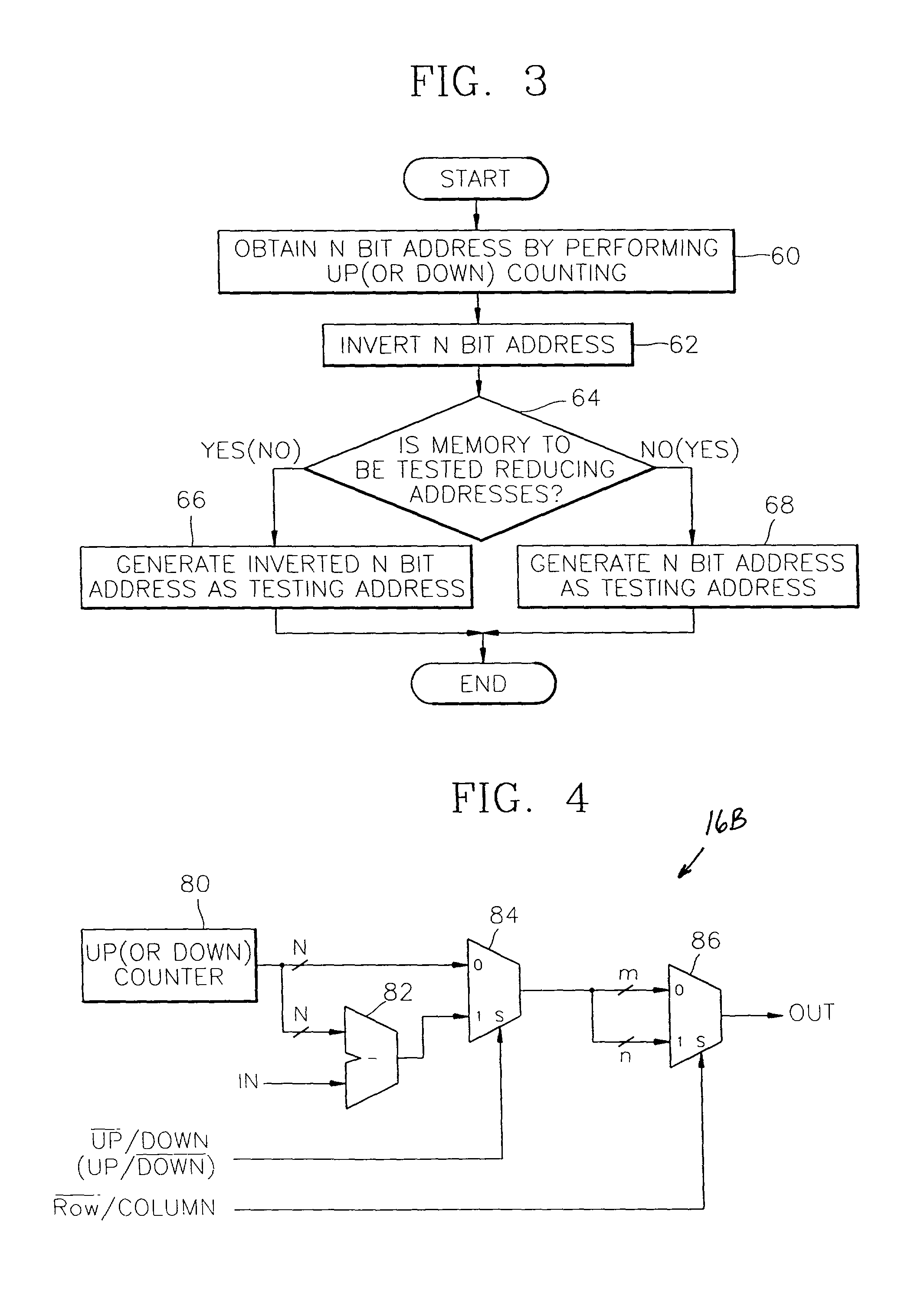
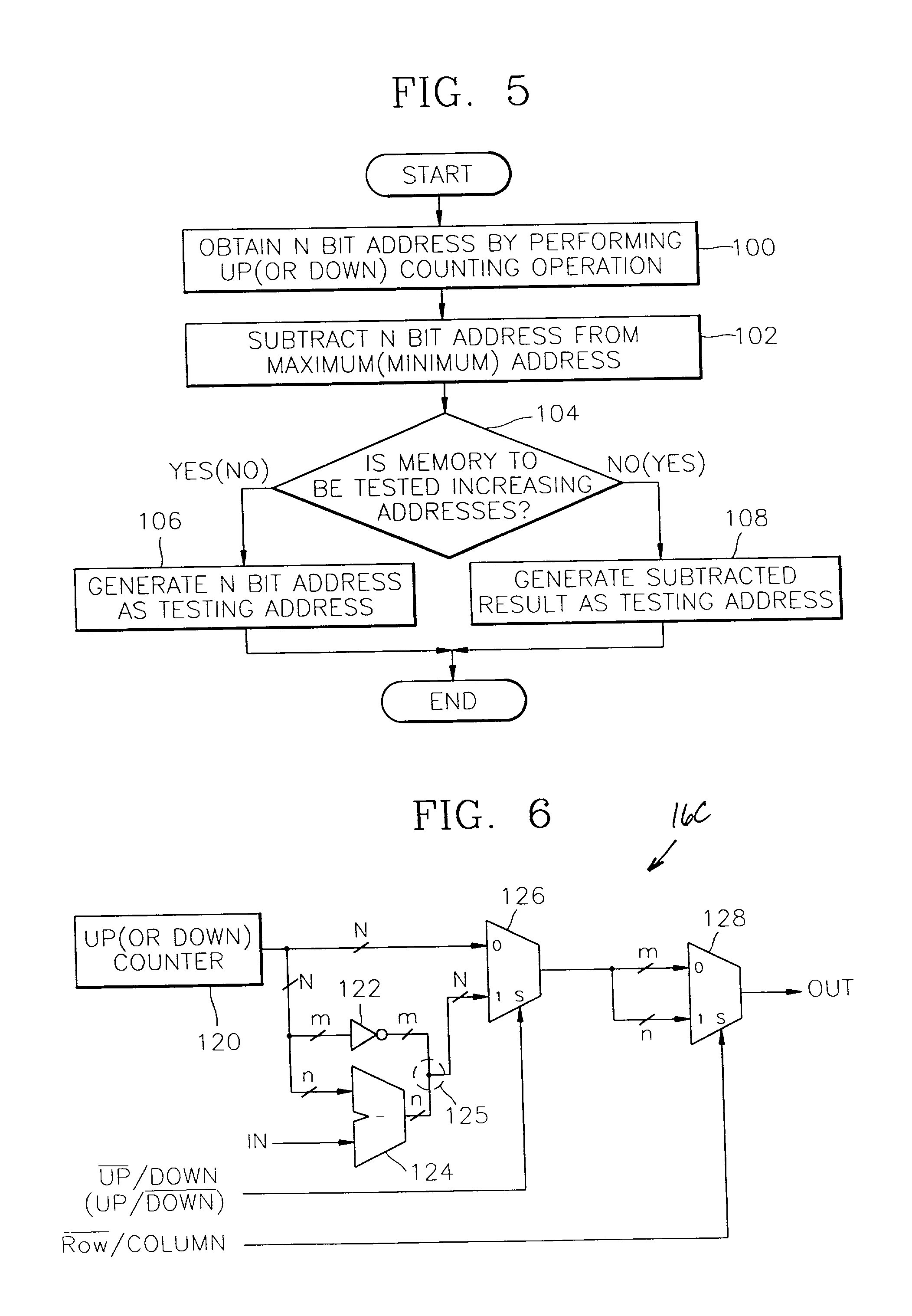
A memory address generating apparatus and method of a dynamic memory testing circuit for generating addresses for testing a dynamic memory which uses all the available addresses of the dynamic memory, which does not use the most significant addresses, and which does not use middle addresses among all the available addresses are provided. The address generator can obtain an up-counted address by up counting the addresses used by the dynamic memory. It can obtain a down-counted address by inverting the N-bit up-counted value, or by subtracting the N-bit up-counted value from the maximum address, or by combining the inverted MSB portion of the N-bit up-counted value with the LSB portion of the N-bit up-counted value subtracted from the LSB portion of the maximum address used in the dynamic memory. The down and up counted addresses are used as addresses for selectively testing the dynamic memory according to a selected testing method.

Description

[0001] 1. Field of the Invention[0002] The present invention relates to testing a memory and more particularly to an address generator of a built-in self test circuit for testing a memory such as a dynamic random access memory (DRAM) and an address generating method thereof.[0003] 2. Description of the Related Art[0004] A built-in self test (BIST) circuit can typically be used as part of a memory testing circuit to test a memory. In a DRAM BIST, the memory to be tested is a DRAM. An address generator in such a BIST circuit is used to generate addresses of the memory to access memory locations to be tested and therefore typically performs many up and down counting operations according to the method being used to test the memory. In the case of an address generator which uses an up / down counter, the size of the circuitry becomes an important consideration since such counters can be very large. Accordingly, it is hard to optimize the area of such devices.[0005] In the case of testing a...

Claims


Application Information

Patent Timeline
Patent Type & Authority Applications(United States)
IPC IPC(8): G06F11/263G11C29/12G11C29/20G01R31/28
CPCG11C29/20G06F11/263
Inventor KIM, HEON-CHEOL
Owner SAMSUNG ELECTRONICS CO LTD
Learn More