Manufacture method of lateral double-diffused transistor
- Summary
- Abstract
- Description
- Claims
- Application Information
AI Technical Summary
Benefits of technology
Problems solved by technology
Method used
Image

Examples
Embodiment Construction
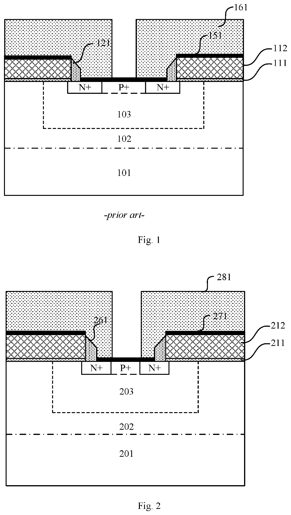
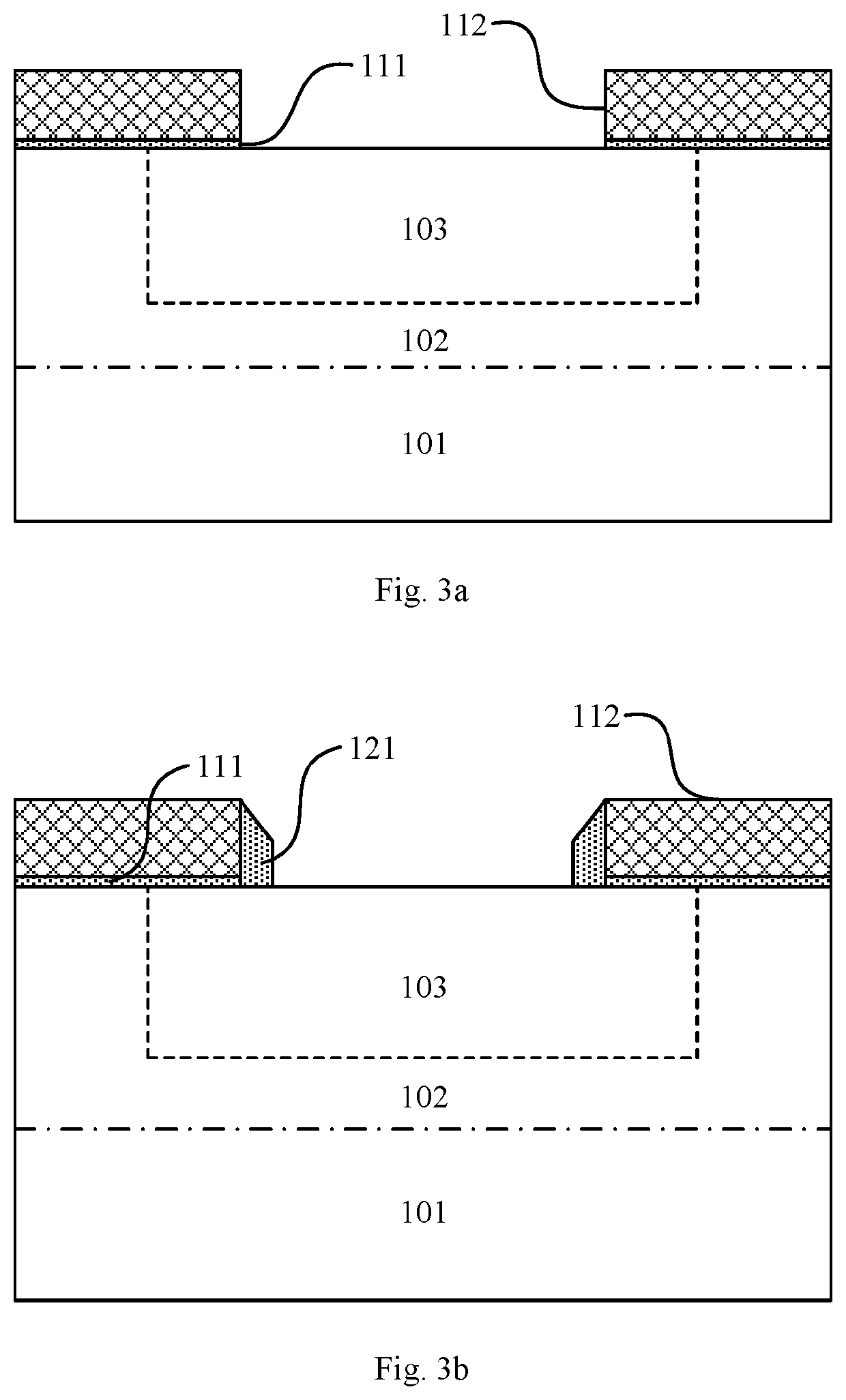
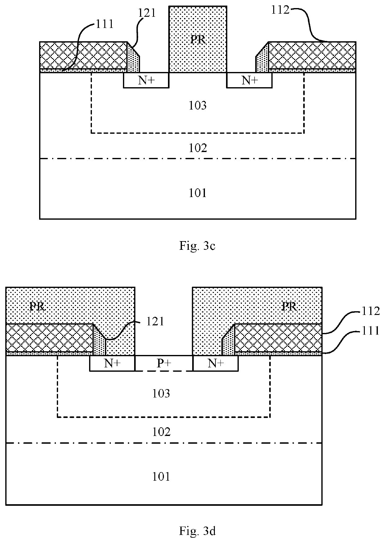
[0037]Various embodiments of the present disclosure will be described in more detail below with reference to the accompanying drawings. In the various accompanying drawings, the same elements are denoted by the same or similar reference numerals. For the sake of clarity, the various portions in the accompanying drawings are not drawn to scale. In addition, some well-known portions may not be shown. For simplicity, a semiconductor structure obtained after several steps may be described in one figure.
[0038]During description of the structure of a device, when a layer or a region is called “on” or “above” another layer or another region, it may be directly on another layer or another region, or other layers or regions are included between it and another layer or another region. In addition, if the device is turned over, the layer and the region will be located “under” or “below” another layer and another region.
[0039]In order to describe the situation of being directly on another layer...
PUM
| Property | Measurement | Unit |
|---|---|---|
| implantation angle | aaaaa | aaaaa |
| width | aaaaa | aaaaa |
| width | aaaaa | aaaaa |
Abstract
Description
Claims
Application Information
 - R&D
- Intellectual Property
- Life Sciences
- Materials
- Tech Scout
- Unparalleled Data Quality
- Higher Quality Content
- 60% Fewer Hallucinations
Browse by: Latest US Patents, China's latest patents, Technical Efficacy Thesaurus, Application Domain, Technology Topic, Popular Technical Reports.
© 2025 PatSnap. All rights reserved.Legal|Privacy policy|Modern Slavery Act Transparency Statement|Sitemap|About US| Contact US: help@patsnap.com