
Die-bonding method and spraying device for LED

a spraying device and die-bonding technology, applied in semiconductor devices, semiconductor/solid-state device details, electrical devices, etc., can solve the problems of deteriorating surface light mixing uniformity and tilting of solid-state wafers

Active Publication Date: 2022-08-16
WUHAN CHINA STAR OPTOELECTRONICS TECH CO LTD
View PDF8 Cites 0 Cited by
  • Summary
  • Abstract
  • Description
  • Claims
  • Application Information

AI Technical Summary

Benefits of technology

The present invention prevents the tilting or short-circuiting of a crystal wafer during the soldering process by spraying solder paste on a pad to form a film. This also prevents the occurrence of faulty soldered-joints caused by white oil between the positive and negative electrodes of the pad, which improves the luminous efficiency of the surface light source and increases the yield of the die-bonding operation.

Problems solved by technology

Due to the application of the solder paste coating, the coating steel mesh used cannot precisely control the amount of solder paste, which causes the solid crystal wafer to tilt due to pulling and dragging of the solder paste during a subsequent reflow process for the solder.
Thereby, the light-emitting direction of the wafer is changed, and the uniformity of light mixing of the surface light source is deteriorated.

Method used


Image

  • Die-bonding method and spraying device for LED
  • Die-bonding method and spraying device for LED
  • Die-bonding method and spraying device for LED

Examples


Embodiment Construction

[0053]The following description of the embodiments is with reference to the drawings and is provided to illustrate the specific embodiments of the invention. The directional terms mentioned in the present invention, such as ‘upper’, ‘lower’, ‘front’, ‘back’, ‘left’, ‘right’, ‘top’, ‘bottom’, etc., are only the directions in the drawings. Therefore, the directional terminology used is for the purpose of illustration and understanding of the invention rather than limiting the invention. In the figures, structurally similar elements are denoted by the same reference numerals.

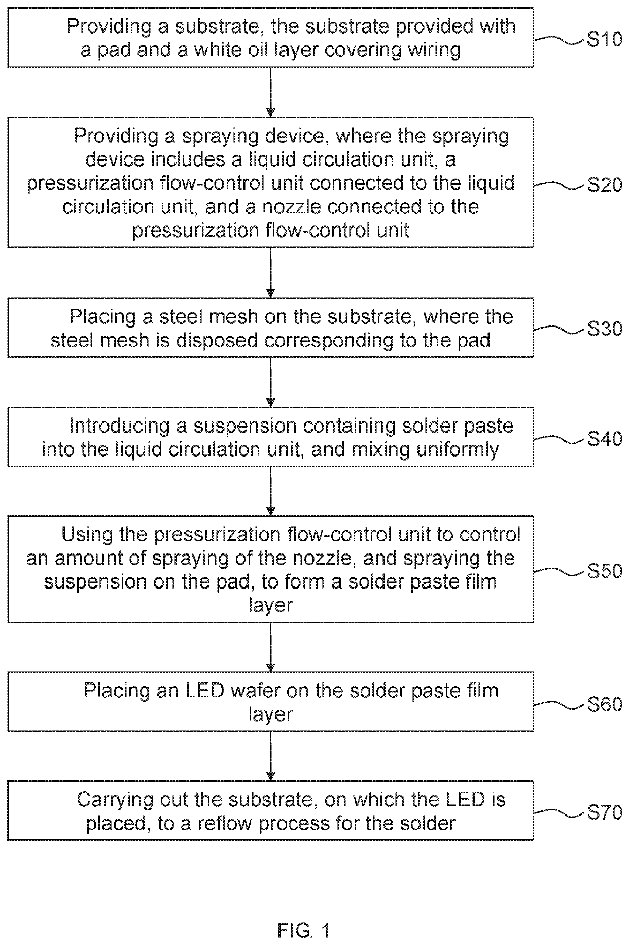
[0054]The invention is directed to the technical problem of the existing die-bonding method for the LED as follows: Due to the solder paste brushing / coating method used for soldering the LED to the pad, the crystal wafer tilts due to pulling and dragging of the solder paste during the subsequent reflow process for the solder; thereby, the light-emitting direction of the wafer is changed, and the uniformity of light...


PUM

PropertyMeasurementUnit
vertical distanceaaaaaaaaaa
areaaaaaaaaaaa
boilingaaaaaaaaaa

Abstract

A die-bonding method and a spraying device for an LED include: providing a substrate provided with a pad and a white oil layer covering wiring, placing a steel mesh on the substrate, and then spraying suspension containing solder paste on the pad by the spraying device, to form a solder paste film layer. Finally, a reflow process for the solder is performed. The solder paste is prepared on the pad by spraying, so that a crystal wafer is prevented from being tilted or short-circuited due to pulling or dragging of the solder paste during the reflow process for the solder, thereby improving uneven brightness of the surface light source.

Description

RELATED APPLICATIONS[0001]This application is a National Phase of PCT Patent Application No. PCT / CN2019 / 091463 having International filing date of Jun. 17, 2019, which claims the benefit of priority of Chinese Patent Application No. 201811270957.2 filed on Oct. 29, 2018. The contents of the above applications are all incorporated by reference as if fully set forth herein in their entirety.FIELD AND BACKGROUND OF THE INVENTION[0002]The present invention relates to the field of LED-packaging technology, and in particular, to a die-bonding method and a spraying device for an LED.[0003]In the die-bonding process of miniLED (mini Light-Emitting Diode), the traditional solder paste coating method is generally used for soldering. Due to the application of the solder paste coating, the coating steel mesh used cannot precisely control the amount of solder paste, which causes the solid crystal wafer to tilt due to pulling and dragging of the solder paste during a subsequent reflow process for...

Claims


Application Information

Patent Timeline
Patent Type & Authority Patents(United States)
IPC IPC(8): H01L33/00H01L23/00
CPCH01L33/0093H01L24/83H01L2224/83815H01L2924/12041H01L33/005H01L33/48H01L21/67126H01L21/6715H01L33/0095H01L33/62H01L2224/81
Inventor YANG, YONG
Owner WUHAN CHINA STAR OPTOELECTRONICS TECH CO LTD
Learn More