
Display device having second electrode including a first portion that is not overlapped with the module hole and a second portion between the module hole and the first portion

a display device and second electrode technology, applied in the direction of organic semiconductor devices, sustainable manufacturing/processing, final product manufacturing, etc., can solve the problems of delamination of the electrode and easy damage by heat and moisture, and achieve the effect of improving durability

Active Publication Date: 2022-06-28
SAMSUNG DISPLAY CO LTD
View PDF11 Cites 0 Cited by
  • Summary
  • Abstract
  • Description
  • Claims
  • Application Information

AI Technical Summary

Benefits of technology

[0004]One or more example embodiments of the present disclosure provide a display device having substantially higher (e.g., improved) durability.
[0005]One or more example embodiments of the present disclosure also provide a method for manufacturing the display device having substantially higher (e.g., improved) durability.

Problems solved by technology

However, when the hole is defined by a physical method, particles are generated from an electrode made of metal to damage a surrounding area, or an electrode is delaminated and easily damaged by heat and moisture.

Method used


Image

  • Display device having second electrode including a first portion that is not overlapped with the module hole and a second portion between the module hole and the first portion
  • Display device having second electrode including a first portion that is not overlapped with the module hole and a second portion between the module hole and the first portion
  • Display device having second electrode including a first portion that is not overlapped with the module hole and a second portion between the module hole and the first portion

Examples


Embodiment Construction

[0037]In this specification, it will also be understood that when one component (or region, layer, portion) is referred to as being cony, ‘connected to’, or ‘coupled to’ another component, it can be directly connected to or coupled to the one component, or an intervening third component may also be present.

[0038]Like reference numerals refer to like elements throughout. Also, in the figures, the thickness, ratio, and dimensions of components are exaggerated for clarity of illustration.

[0039]The term “and / or” includes any and all combinations of one or more of the associated listed items.

[0040]It will be understood that, although, the terms such as ‘first’ and ‘second’ are used herein to describe various elements, these elements should not be limited by these terms. The terms are only used to distinguish one component from other components. For example, a first element referred to as a first element in one embodiment can be referred to as a second element in another embodiment withou...


PUM

PropertyMeasurementUnit
temperatureaaaaaaaaaa
areaaaaaaaaaaa
standard reduction potentialaaaaaaaaaa

Abstract

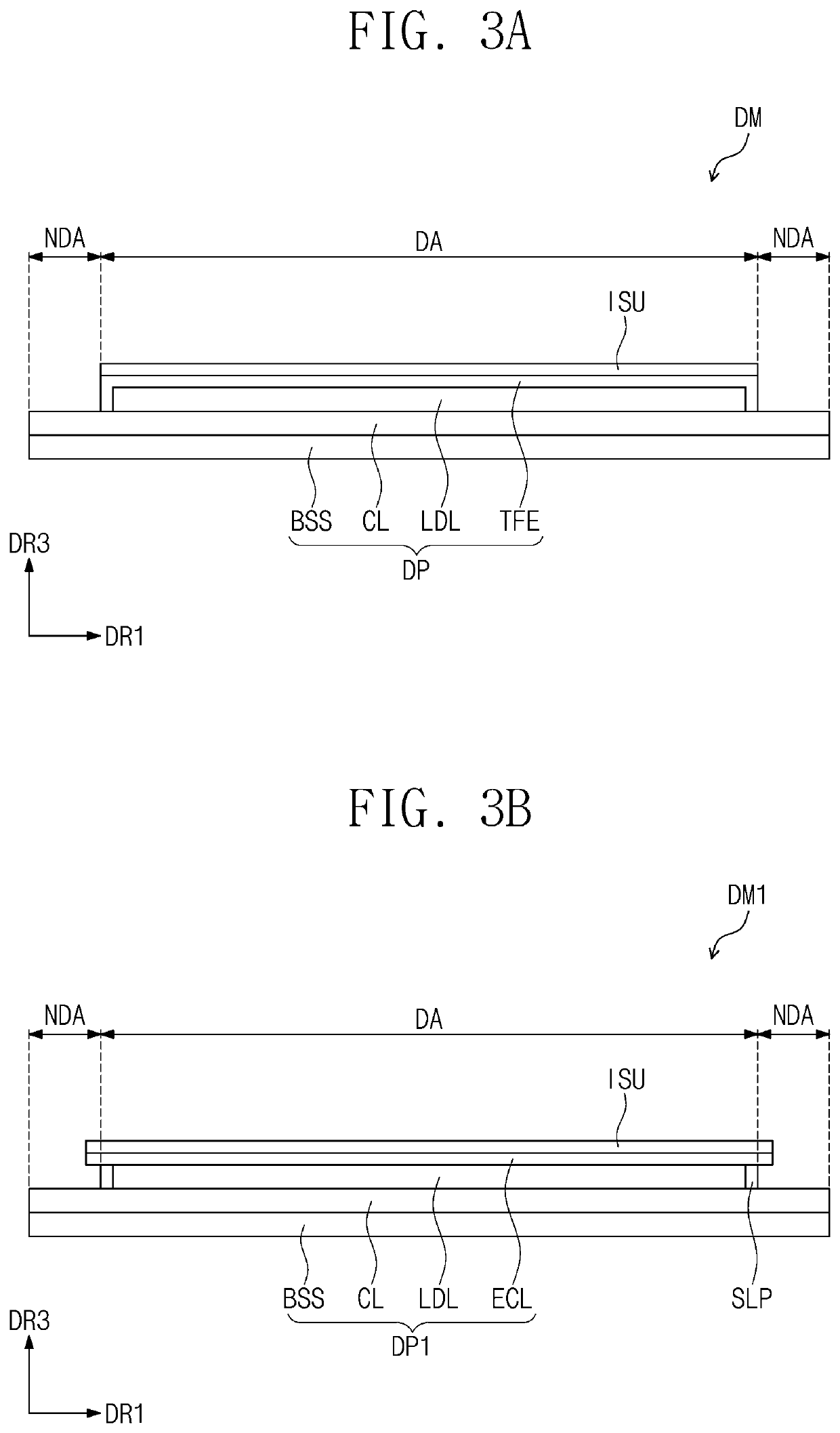
A display device according to an embodiment may include a base substrate, a circuit layer, a light emitting element layer, and a module hole. The light emitting element layer may include a first electrode, a light emitting layer, and a second electrode. The second electrode may include a first portion that is not overlapped with the module hole and has a first thickness and a second portion between the module hole and the first portion and having a thickness that gradually increases in a direction toward the first portion. Thus, the display device may improve in durability in a hot and humid environment.

Description

CROSS-REFERENCE TO RELATED APPLICATIONS[0001]This application claims priority to and the benefit of Korean Patent Application Nos. 10-2019-0053958, filed on May 8, 2019, and 10-2019-0123805, filed on Oct. 7, 2019, the entire contents of both of which are hereby incorporated by reference.BACKGROUND1. Field[0002]The present disclosure relates to a display device and a method for manufacturing the same, and more particularly, to a display device having improved durability and a method for manufacturing the same.2. Description of the Related Art[0003]In recent years, in order to accommodate an electronic module such as a camera in a display device, a technique for defining a hole passing through a display area of a display module has been actively researched. However, when the hole is defined by a physical method, particles are generated from an electrode made of metal to damage a surrounding area, or an electrode is delaminated and easily damaged by heat and moisture.SUMMARY[0004]One o...

Claims


Application Information

Patent Timeline
Patent Type & Authority Patents(United States)
IPC IPC(8): H01L51/52H01L27/32H01L51/00H01L51/56
CPCH01L51/5225H01L27/323H01L27/3244H01L51/0023H01L51/0096H01L51/5253H01L51/56H01L2227/323H01L2251/301H10K59/123H10K59/1213H10K59/1315H10K59/122H10K59/1201H10K71/00Y02E10/549Y02P70/50H10K59/00H10K59/12H10K50/813H10K50/822H10K2102/351H10K50/844H10K59/40H10K71/621H10K77/10H10K2102/00
Inventor CHOI, YUNJUNGKIM, SANGYEOLNOH, SOKWONKIM, HYUNGSIKOH, SUHYUN
Owner SAMSUNG DISPLAY CO LTD
Learn More