Thermally activated delayed fluorescence material, organic electroluminescent device, and display panel

a technology of delayed fluorescence and organic electroluminescent devices, which is applied in the direction of organic chemistry, luminescent compositions, semiconductor devices, etc., can solve the problems of limited application of fluorescent electroluminescent devices, lack of green light-emitting materials, and inability to achieve maximum internal quantum efficiency (iqe) of fluorescence materials, etc., to achieve the effect of increasing the synthesis efficiency of green light-emitting tadf materials

Active Publication Date: 2022-03-22
WUHAN CHINA STAR OPTOELECTRONICS SEMICON DISPLAY TECH CO LTD
View PDF1 Cites 3 Cited by
  • Summary
  • Abstract
  • Description
  • Claims
  • Application Information

AI Technical Summary

Benefits of technology

[0009]An object of the present invention is to provide a thermally activated delayed fluorescence (TADF) materially, in particular a green light-emitting TADF material. Specifically, in the present invention, a green light-emitting TADF material having small energy gap between the lowest singlet and triplet excited states (ΔEST), high photoluminescence quantum yield (PLOY), and fast reverse intersystem crossing (RISC) is provided. Furthermore, the green light-emitting TADF material is applied to an organic light-emitting layer of an organic electroluminescent device to obtain a series of high-efficiency organic light-emitting diodes (OLEDs
[0031]In the present invention, a green light-emitting TADF material having significantly characteristics of TADF material is provided by matching different functional groups. In addition, the present invention provides a reasonable synthesis route to increase synthesis efficiency of the green light-emitting TADF material. The green light-emitting TADF material provided by the present invention can be used in an organic light-emitting layer, thereby realizing a series of high-performance and high-efficiency TADF electronic devices. Furthermore, the green light-emitting TADF material can be applied to a display panel.

Problems solved by technology

The OLED devices based on the fluorescence materials can only achieve 25% internal quantum efficiency (IQE) at most because the branching ratio of singlet and triplet excitons is 1:3 in the OLED devices.
As a result, applications of fluorescent electroluminescent devices are limited.
Furthermore, the lack of green light-emitting materials is a bottleneck of the phosphorescent materials.
Nowadays, compared to the phosphorescent materials, there is a lack of TADF materials satisfying the above required conditions.
Moreover, not only the phosphorescent materials but the TADF materials are lacking in green light-emitting materials.

Method used


Image

  • Thermally activated delayed fluorescence material, organic electroluminescent device, and display panel
  • Thermally activated delayed fluorescence material, organic electroluminescent device, and display panel
  • Thermally activated delayed fluorescence material, organic electroluminescent device, and display panel

Examples


first embodiment

re of Compound Represented by Formula (1)

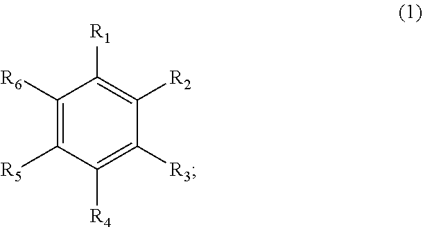
[0040]In the present embodiment, specific structure of compound represented by formula (1) is described by table (1). A thermally activated delayed fluorescence (TADF) material provided by the present invention includes a compound represented by the following structural formula (1):

[0041]

[0042]

Table 1numeralsstructural formula  1 2 3 4 5 6 7 8 910111213

wherein D is an electron donor group represented by the following formula (D-i), and A is an electron acceptor group represented by the following structural formula (A-i-52):

[0043]

and

wherein X is fluorine.

second embodiment

rocess of Compound 1

[0044]In the present embodiment, a TADF material is provided including compound 1 represented by the following structural formula (I-1):

[0045]

[0046]Synthesis of compound 1 is illustrated bellow:

[0047]

[0048]Specific synthesizing process is illustrated below:

[0049]step 1: Adding raw material 1 (2.67 g, 5 mmol), phenoxazine (1.1 g, 6 mmol), palladium acetate (45 mg, 0.2 mmol), and tri-tert-butylphosphine tetrafluoroborate (0.17 g, 0.6 mmol) into a two-neck bottle. Then, placing the two-neck bottle in a closed environment and adding NaOt-Bu (0.58 g, 6 mmol) into the two-neck bottle. Then, adding water- and oxygen-free toluene (40 ml) into the two-neck bottle in argon environment at 120 degrees Celsius for 24 hours to form a reacting solution.

step 2: adding the reacting solution into cold water after the reacting solution reaches to room temperature. Extracting organic phase from the reacting solution for three times by dichloromethane. Combining the organic phase ext...

third embodiment

Process of Compound 2

[0050]In the present embodiment, a TADF material is provided including compound 2 represented by the following structural formula (I-2):

[0051]

[0052]Synthesis of compound 2 is illustrated bellow:

[0053]

[0054]Specific synthesizing process is illustrated below:

[0055]step 1: Adding raw material 2 (2.67 g, 5 mmol), phenoxazine (1.1 g, 6 mmol), palladium acetate (45 mg, 0.2 mmol), and tri-tert-butylphosphine tetrafluoroborate (0.17 g, 0.6 mmol) into a 100 ml two-neck bottle. Then, placing the two-neck bottle in a closed environment and adding NaOt-Bu (0.58 g, 6 mmol) into the two-neck bottle. Then, adding water- and oxygen-free toluene (40 ml) into the two-neck bottle in argon environment at 120 degrees Celsius for 24 hours to form a reacting solution.

step 2: adding the reacting solution into cold water (200 ml) after the reacting solution reaches to room temperature. Extracting organic phase from the reacting solution for three times by dichloromethane. Combining the ...


PUM

PropertyMeasurementUnit
IQEaaaaaaaaaa
IQEaaaaaaaaaa
thermally activated delayed fluorescenceaaaaaaaaaa

Abstract

A thermally activated delayed fluorescence (TADF) material including a compound represented by formula (I). The TADF material can be applied to an organic light-emitting layer, thereby realizing a series of high-performance TADF electronic devices.

Description

RELATED APPLICATIONS[0001]This application is a National Phase of PCT Patent Application No. PCT / CN2019 / 092074 having International filing date of Jun. 20, 2019, which claims the benefit of priority of Chinese Patent Application No. 201910098498.2 filed on Jan. 31, 2019. The contents of the above applications are all incorporated by reference as if fully set forth herein in their entirety.FIELD AND BACKGROUND OF THE INVENTION[0002]The present invention relates to a field of organic electroluminescent technology and, more particularly, to a thermally activated delayed fluorescence material, an organic electroluminescent using same, and a display panel using same.[0003]Organic light-emitting diodes (OLEDs) are exceptional in terms of self-illumination, luminescence efficiency, viewing angles, response times, temperature adaptation ranges, manufacturing process, drive voltage, power consumption, body type, flexibility, and application prospect. Therefore, the OLEDs have been spotlighte...

Claims


Application Information

Patent Timeline
Patent Type & Authority Patents(United States)
IPC IPC(8): H01L51/50H01L51/00C07D413/10C09K11/06H01L51/52
CPCH01L51/0072C07D413/10C09K11/06H01L51/0035H01L51/0036H01L51/0037H01L51/0067H01L51/0071C09K2211/1018H01L51/5016H01L51/5056H01L51/5072H01L51/5088H01L51/5092H01L51/5206H01L51/5221H01L2251/301H01L2251/308H10K85/657H10K85/6572H10K50/11H10K2101/20H10K85/111H10K85/113H10K85/654H10K85/1135H10K50/15H10K50/16H10K50/17H10K50/81H10K50/82H10K50/171H10K2101/10H10K2102/00H10K2102/103
Inventor BAI, YAMEILI, XIANJIEHUANG, JINCHANGGU, YUYANG, LINLUO, JIAJIA
Owner WUHAN CHINA STAR OPTOELECTRONICS SEMICON DISPLAY TECH CO LTD
Why Eureka
Try Eureka