Oscillator and imaging device
a technology of oscillator and imaging device, which is applied in the direction of oscillator generator, electrical apparatus, etc., can solve the problems of stability of suppression of parasitic oscillation and need for oscillator to continue to consume power, and achieve the effect of reducing power consumption
- Summary
- Abstract
- Description
- Claims
- Application Information
AI Technical Summary
Benefits of technology
Problems solved by technology
Method used
Image

Examples
first embodiment
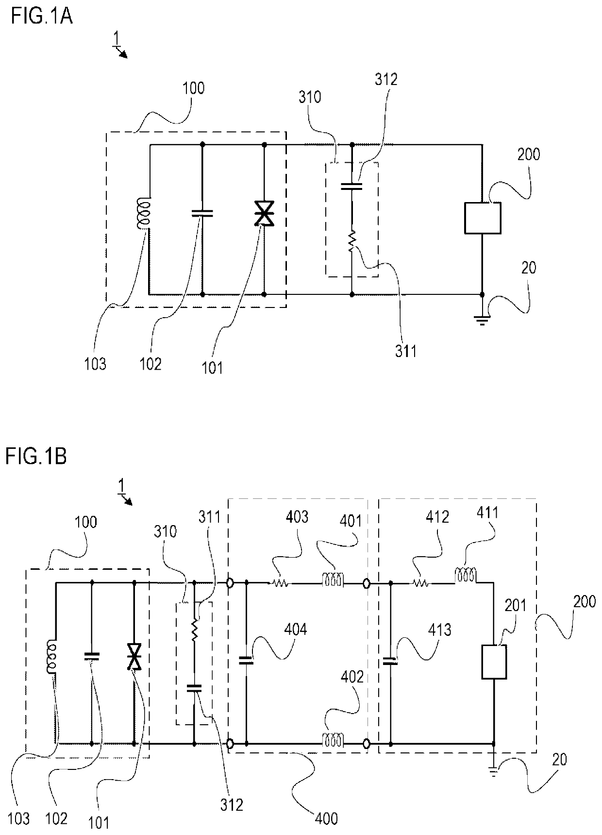
[0036]An oscillator according to the present embodiment includes a voltage bias circuit that applies a voltage to a negative resistance element. The negative resistance element and a shunt element in which a resistor and a capacitor are arranged in series are electrically connected in parallel to the voltage bias circuit. This realizes an oscillator that is capable of providing stable suppression of parasitic oscillation while preventing an increase in power consumption.
[0037]Circuit Configuration of Oscillator
[0038]A circuit configuration of an oscillator 1 according to the present embodiment will be described with reference to FIGS. 1A and 1B. FIG. 1A illustrates a simple circuit configuration (minimum circuit configuration) of the oscillator 1, and FIG. 1B illustrates a more detailed circuit configuration of the oscillator 1. The oscillator 1 includes an oscillation circuit 100, a voltage bias circuit 200, and a shunt element 310.
[0039]The oscillation circuit 100 is a resonator (...
second embodiment
[0089]An oscillator 2 according to a second embodiment is the same as the oscillator 1 according to the first embodiment except for the number of shunt elements and their arrangement place. The oscillator 2 according to the present embodiment will be described below with reference to FIG. 8. In the oscillator 2 according to the present embodiment, two shunt elements are formed on different members (the chip and the printed circuit board).
[0090]The oscillator 2 includes a shunt element 520 on the printed circuit board 500 in addition to the printed circuit board 500, the package 501, the chip 600, and the voltage bias circuit 200 included in the oscillator 1 according to the first embodiment.
[0091]The chip 600 includes a capacitive element 302 as a shunt element in place of the shunt element 310 of the first embodiment. The capacitive element 302 is designed such that the length of the wire connecting the capacitive element 302 and the oscillation circuit 100 (negative resistance ele...
third embodiment
[0100]In the oscillator 2 according to the second embodiment, the shunt element 520 is formed on the printed circuit board 500. However, in an oscillator 3 according to a third embodiment, the shunt element 520 is formed in the package 501 as illustrated in a circuit configuration diagram of FIG. 10A. The following description for the oscillator 3 according to the third embodiment will focus on different parts from the second embodiment with reference to FIGS. 11A and 11B.
[0101]FIG. 11A is a schematic diagram illustrating the oscillator 3 of the present embodiment. The package 501 includes pins 503, and the printed circuit board 500 includes a pin socket 504 for the pins 503. Accordingly, the package 501 including the chip 600 can be inserted into and removed from the printed circuit board 500 as illustrated in FIG. 11B. Thus, in a case where a user desires to change the characteristics of the oscillator 3 or in a case where the oscillator 3 breaks down and needs to be replaced, it ...
PUM
 Abstract
Description
Claims
Application Information
 - R&D
- Intellectual Property
- Life Sciences
- Materials
- Tech Scout
- Unparalleled Data Quality
- Higher Quality Content
- 60% Fewer Hallucinations
Browse by: Latest US Patents, China's latest patents, Technical Efficacy Thesaurus, Application Domain, Technology Topic, Popular Technical Reports.
© 2025 PatSnap. All rights reserved.Legal|Privacy policy|Modern Slavery Act Transparency Statement|Sitemap|About US| Contact US: help@patsnap.com