Display device

a technology of display device and display panel, which is applied in the direction of semiconductor devices, electrical equipment, instruments, etc., can solve the problems of heat generated by sealing process and affect other elements of the display, and achieve the effect of suppressing or substantially preventing heat generated in sealing process and reducing or preventing shrinkage of pixels due to outgasing of organic insulating layers

Active Publication Date: 2021-05-18
SAMSUNG DISPLAY CO LTD
View PDF14 Cites 2 Cited by
  • Summary
  • Abstract
  • Description
  • Claims
  • Application Information

AI Technical Summary

Benefits of technology

[0007]Aspects of embodiments of the present invention are directed to a display device capable of reducing or preventing damage caused by heat generated in a sealing process.
[0028]According to the exemplary embodiments, the heat generated in the sealing process is suppressed or substantially prevented from being conducted to the organic insulating layer, so that shrinkage of the pixel due to outgasing of the organic insulating layer can be reduced or prevented.

Problems solved by technology

Recently, there has been an increasing demand for reducing a width of the bezel, which reduces a distance between a display area and a sealant, and causes heat generated by a sealing process to affect other elements of the display.

Method used


Image

  • Display device
  • Display device
  • Display device

Examples


Embodiment Construction

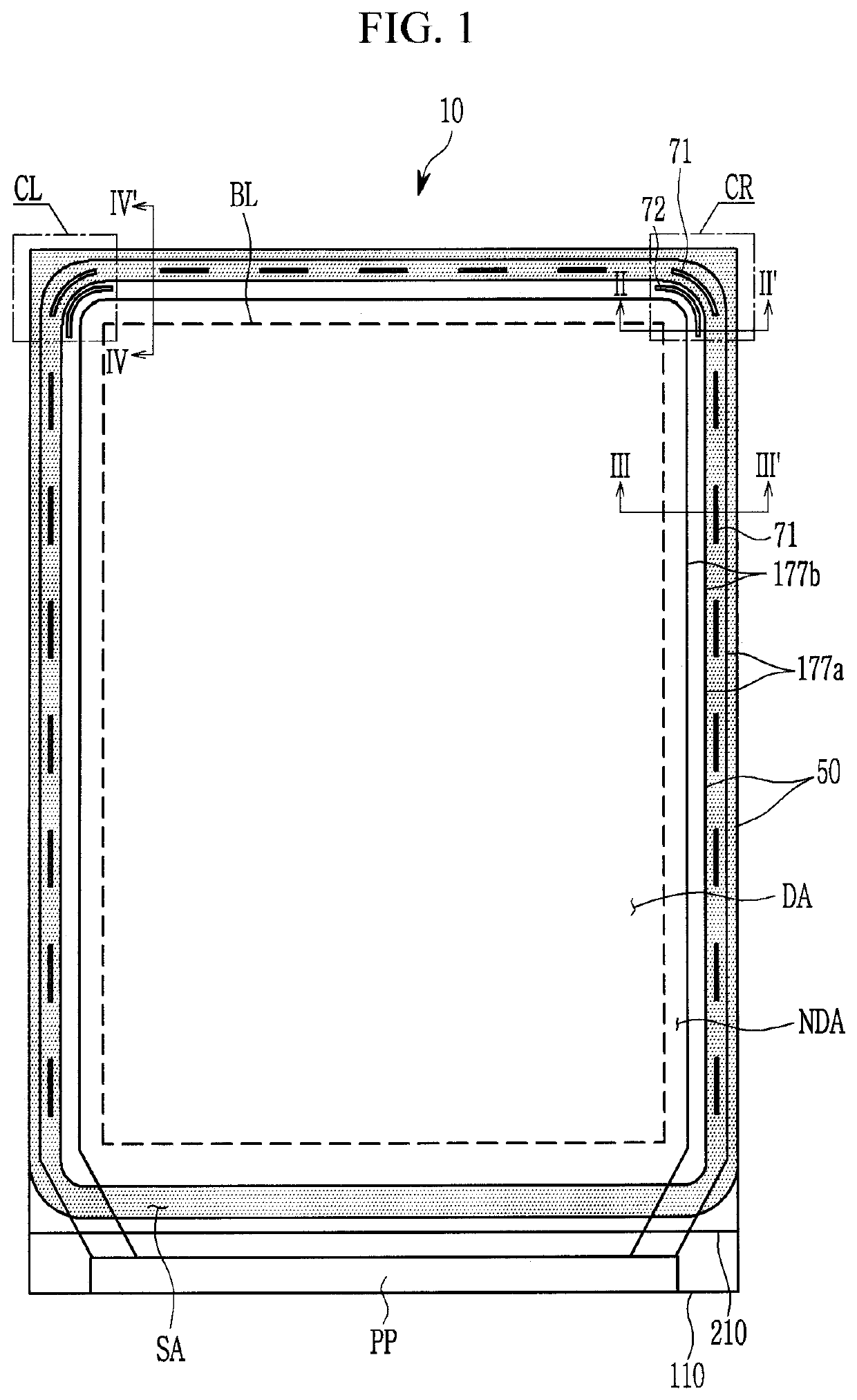
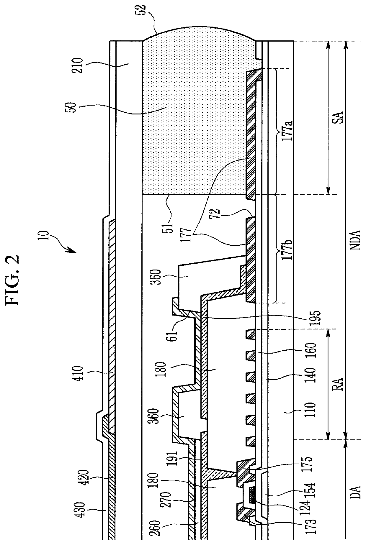
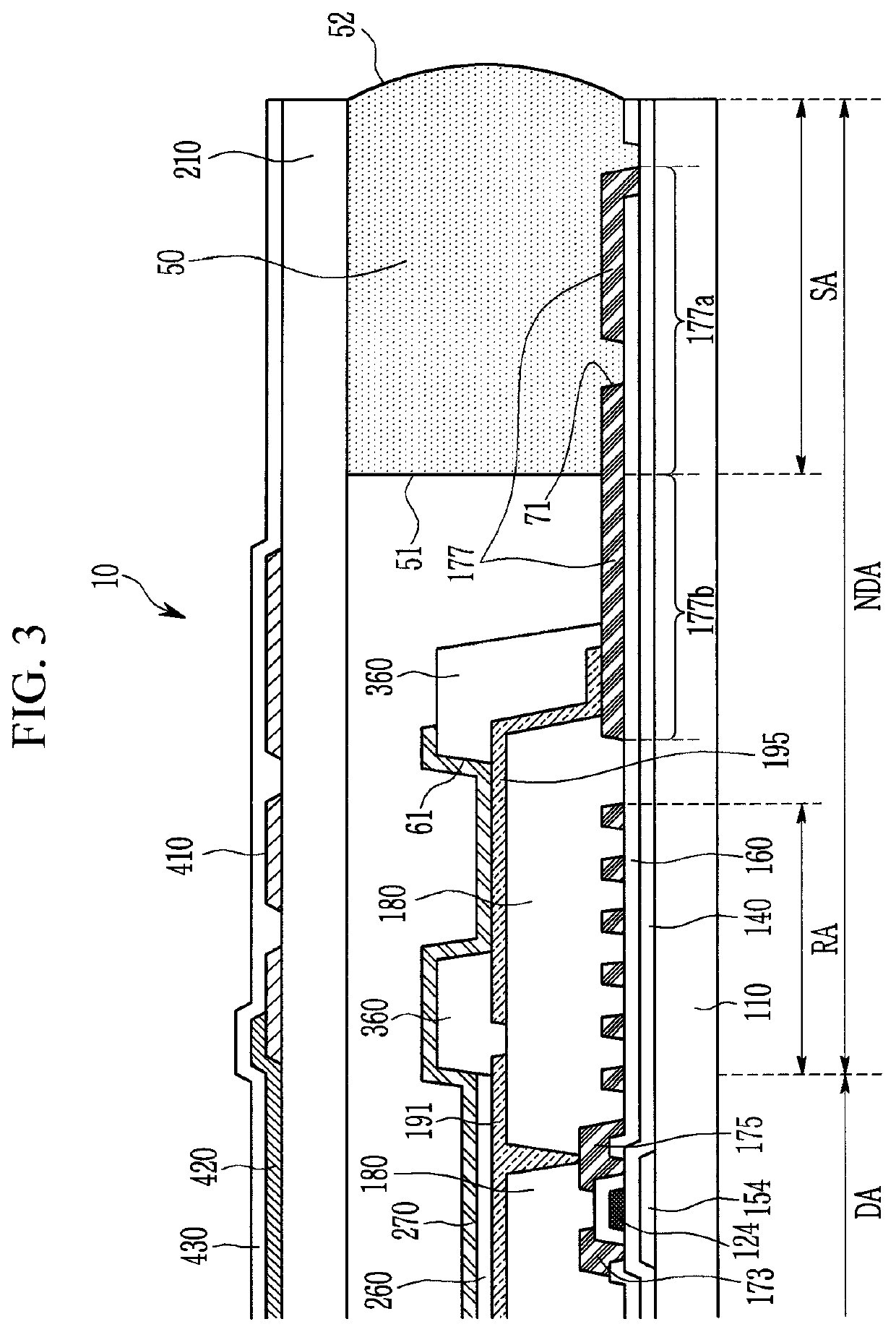
[0039]The present invention will be described more fully hereinafter with reference to the accompanying drawings, in which exemplary embodiments of the invention are shown. As those skilled in the art would realize, the described embodiments may be modified in various suitable ways, all without departing from the spirit or scope of the present invention.

[0040]To clearly describe the present invention, parts that are not critical to the description may be omitted. Herein, like numerals refer to like or similar constituent elements throughout the specification.

[0041]Further, because sizes and thicknesses of constituent members shown in the accompanying drawings are arbitrarily given for better understanding and ease of description, the present invention is not limited to the illustrated sizes and thicknesses. In the drawings, the thickness of layers, films, panels, regions, etc., may be exaggerated for clarity.

[0042]Next, a display device according to an exemplary embodiment of the pr...


PUM

PropertyMeasurementUnit
DAaaaaaaaaaa
areaaaaaaaaaaa
voltageaaaaaaaaaa

Abstract

A display device includes a first substrate having a display area and a non-display area around the display area, a light-emitting element in the display area and including a pixel electrode, a common electrode, and an emission member between the pixel electrode and the common electrode, a common voltage transfer line in the non-display area and electrically connected to the common electrode, a second substrate opposite the first substrate, and a sealant in the non-display area between the first substrate and the second substrate, the sealant surrounding the display area, wherein the common voltage transfer line includes a first portion overlapping the sealant and a second portion positioned between the sealant and the display area, and wherein the second portion has at least one opening or cut-out portion.

Description

CROSS-REFERENCE TO RELATED APPLICATION[0001]This application claims priority to and the benefit of Korean Patent Application No. 10-2017-0062446, filed in the Korean Intellectual Property Office on May 19, 2017, the entire content of which is incorporated herein by reference.BACKGROUND1. Field[0002]Aspects of this disclosure relate to a display device, and more particularly, to an organic light emitting diode display.2. Description of the Related Art[0003]An organic light emitting diode display includes pixels implemented by organic light emitting diodes each including two electrodes and an organic emission layer disposed therebetween. Electrons injected from a cathode that is one electrode of the organic light emitting diode and holes injected from an anode that is another electrode are bonded to each other in the organic emission layer to form excitons, and light is emitted while the excitons discharge energy. The organic light emitting diode display may display an image by contro...

Claims


Application Information

Patent Timeline
Patent Type & Authority Patents(United States)
IPC IPC(8): H01L51/56G09G3/3258H01L27/32H01L51/52
CPCH01L51/5246G09G3/3258H01L27/3276H01L51/56G02F2201/121G02F2201/123H10K59/131H10K50/8426H10K59/40H10K59/122H10K71/00
Inventor KWON, SUN-JAKWAK, WON KYUKIM, DONG WOOKKIM, HAN SOOSHIN, AE
Owner SAMSUNG DISPLAY CO LTD
Why Eureka
Try Eureka